sábado, 17 de julio de 2010

Monolithic VCO tackles triple bands

Trimming the single-chip PLL + VCO solution introduced last spring, National Semiconductor Corp. has developed a new family of monolithic RF voltage-controlled oscillators (VCOs). The first member of this new line of integrated VCOs is aimed at handling triple bands in the cellular arena. The LMX2604 is tailored to meet the specifications for the GSM and GPRS cellular standards. In fact, the small form factor and low phase noise of the device are designed for GSM900/DCS1800/PCS1900 triple-band applications.


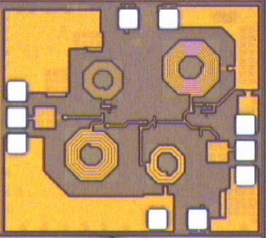
In essence, the LMX2604 chip incorporates two VCOs, one for GSM in the 880 MHz to 915 MHz range and a second one for DCS in the 1710 MHz to 1785 MHz band and PCS in the 1850 to 1910 MHz band. In addition, it offers two separate buffer amplifiers to drive an external high-power amplifier, one for the GSM900 band and the other for DCS1800/PCS1900 bands. Furthermore, the monolithic VCO provides a differential buffer amplifier to drive the mixer in offset PLL (see the figure). The resonant circuits of the VCOs are fully integrated on the chip to ease the application of the IC. The oscillator core and the tank circuit are designed to be immune to external noise such as supply and load variations. According to the manufacturer, the high quality factor of the embedded tank circuit achieves very low phase noise characteristics at the VCO output. It has low phase noise of -167 dBc/Hz at 20 MHz offset in the GSM band, and -162 dBc/Hz at 20 MHz offset in the DCS and PCS bands. The only required external components are a couple of supply bypass capacitors and matching components. A control pin for controlling the oscillation frequency is shared by the two VCOs. The new VCO exploits 0.25 µm RF CMOS process for integration.

High output power for the integrated VCO is +6 dBm in all bands, which is ideal for use with transmit closed-loop modulation. The LMX2604 also has 2.7 V to 3.3 V operation and low current consumption of 18 mA in GSM mode and 15 mA in DCS/PCS mode. Other salient features of the device include smaller package and fewer external components. To provide a smaller package than alternative triple-band VCO modules, the LMX2604 is housed in a 20-pin leadless leadframe package (LLP), which is 4 × 4 mm in size. This allows designers to save significant board space in mobile handsets. The supplier also has plans to offer additional members in this line throughout the year. Available now, it is priced at $1.35 in 1,000 units.

Publicado por: Jahir Alonzo Linares Mora C.I: 19769430 CRF
Bibliografia: http://rfdesign.com/vlf_to_uhf/rf_circuits/radio_monolithic_vco_tackles/


Commercial-off-the-shelf MMIC components offer high reliability

Demands on reliability of commercial-off-the-shelf (COTS) components are increasing. Responding to this need, Mini-Circuits has instituted rigorous new design guidelines and reliability inspection verifications to ensure Mini-Circuits components will last longer than the lifetime of the customer's end product. This paper presents the details of design and quality assurance programs, which will help designers decide on incorporating COTS components into their military or other high-reliability applications.

The life of semiconductor products is a function of junction temperature. The hotter the junction gets, the shorter will be the life. Unless a product is properly designed, no amount of testing will ensure reliability. Packaging materials should include specially developed lead frames and highly heat-conductive die-bond epoxies and mold compounds to efficiently dissipate heat.

Die designers need to ensure low junction temperature by:
  • Using bigger devices or several small devices connected in parallel to spread the heat.
  • Laying out the die so as to physically separate the heat-generating elements.

Using bigger devices tends to degrade high-frequency performance. With smaller devices in parallel, one needs to ensure that power is combined in such a way that manufacturing tolerance does not favor current flow in one device over another, as this can result in overheating and thermal runaway.

Theoretical prediction of junction temperature is the first step in the design. Three-dimensional finite element modeling of the die and package is one of the methods used to analyze heat distribution and predict hot spot temperatures.

After the die is manufactured, it is packaged. Packaged devices are selectively etched to expose the die while retaining the mechanical integrity of the device. High-resolution infrared images are then taken to validate the thermal predictions. Figure 1 shows the infrared thermal image of a medium-power gain block amplifier.

Figure 1

This image is taken with the device package mounted on a base plate with temperature held at 85° C, which is the highest specified ambient operating temperature of the device. It is a good practice to add another 5° C or 10° C to this temperature to account for the temperature rise of the user's printed circuit board (PCB) over the ambient. Most of the dice are designed to have hot spot temperature less than 130° C at the highest specified ambient.

Important information required for mean time to failure (MTTF) prediction is the relationship of MTTF to hot spot temperature. Standard industry practice is to perform accelerated life tests to derive this relationship. Circuit designers should, therefore, use the device-specific MTTF graph given in data sheets (example: Figure 2), instead of general prediction models such as MIL-HDBK-217 (reliability prediction of electronic equipment). Those models tend to give overly pessimistic values for modern commercial semiconductor devices.

Figure 2

Figure 2 shows MTTF vs. junction temperature for HBT devices such as Mini-Circuits ERA and Gali series amplifiers as an example. Note the MTTF of the device shown in Figure 1 is about 500 years at 85° C ambient temperature, which is adequate for most applications. To increase reliability, lower device current needs to be used (readily accomplished as this is a current-controlled amplifier) at the expense of lower output power.

 Package design and reliability verification

Vapor pressure of moisture inside a non-hermetic package increases greatly when the package is exposed to moisture followed by the high temperature of solder reflow[3].

A proprietary technique has been developed to prevent delamination, after years of research, and has been qualified to meet J-STD-020C.

A scanning acoustic microscope (SAM) is used during qualification and process monitoring to detect delamination. The operation of SAM is based on simple acoustic principles. The devices under examination are submerged in a large container of de-ionized water. An ultrasonic transducer is placed near the surface of the device below the water line. The transducer generates a series of high-frequency waves that impinge upon the various package components. The acoustic wave will penetrate, and will be reflected fully or partially based on the nature of the material; the transducer detects the reflections. Based on the amplitudes and the phases of the reflected waves, the acoustic microscope can detect internal package cracks, die cracks, tilted die, voids in the die attach and interface delaminations.

Table 1 lists the tests, criteria, standard and sample size used. Figure 3 is a flow chart of the tests. Peak reflow temperature in the moisture sensitivity level (MSL) test is 260° C, which corresponds to the peak reflow temperature used with lead-free solders.

Figure 3

Figure 4a shows SAM images of an array of units of conventional design that have undergone MSL tests per Table 1. Red indicates delamination. Note 20 of 22 units have delamination.

Figure 4a

Figure 4b shows the SAM image of an array of units of improved design, which have undergone MSL tests per Table 1. No unit failed.

Figure 4b

JEDEC spec[3] allows certain types of delaminations as long as the units pass electrical tests. Our criterion for success is units should pass the moisture absorption tests and C-SAM to show no voids at all. Voids affect thermal resistance as heat is dissipated from the junction to the ambient through the package. Most of the heat is dissipated through the die onto the lead frame on which it sits. Thus, the improved design package is of great value for applications requiring the devices to perform reliably for a long period of time, such as for the military.

Thermometer inside

Diode forward voltage varies with temperature. This characteristic is used to measure die hot spot temperature for each lot. For each MMIC amplifier product, a special die is designed that has a thermal-sensing diode close to the die hot spot. This die is part of each reticle and will, therefore, undergo similar process variations as the regular die under investigation. The special die is packaged and powered, a small current is passed through the diode, and diode voltage is measured to determine the hot spot temperature. Figure 5 shows hot spot temperature of a typical device. This type of quality assurance test ensures the thermal resistance is a parameter of concern, and any change will trigger a review and process changes if required to bring it under control.

Figure 5

Extended HTOL tests

Some manufacturers subject samples to life tests at maximum specified ambient temperature for 1000 hours. We use 125° C ambient, which is 40° C above the 85° C maximum ambient specified, and which is also used by other quality-conscious manufacturers. What distinguishes Mini-Circuits is the use of extended life test for 5000 hours instead of 1000 hours. This tough life test would bring out defects that ordinarily would not be caught. The disadvantage of this process is that it takes a long time to correct design defects. In order to minimize design cycle time, small manufactured lots go through these tests and results are used to correct the design of production lots.
X-ray inspection

X-ray equipment is used in the assembly process as a process control monitor to look for wire sweeps at molding or wire bond defects. Figure 6 shows an assembly defect. Such information is used for applying corrections to manufacturing processes in real time.

Figure 6

S-parameter tests for each manufacturing lot

Most manufacturers test S-parameters during qualification on one sample, and rarely on a few samples, irrespective of the production quantities. Production tests are at spot frequencies and for few parameters such as gain and dc current.

At Mini-Circuits, we believe variations need to be continuously monitored. For this purpose, each manufacturing lot of the devices undergoes full S-parameter tests. The data is compared to a golden sample from the original qualification lot. This enables a tight process control on variations of parameters that may affect our customers' applications. Figures 7 and 8 are examples of plots obtained

Figure 7

 Figure 8

Qualification tests

Industry-standard qualification tests are done in addition to the aforementioned tests. These include HTOL, HAST, vibration and shock, and thermal cycling and satisfy traditional qualification requirements of the industry.
Conclusion

Demands on quality of very high volume commercial products exceed the requirements specified for most military products.

Extensive reliability and physical analysis capabilities at the assembly operations such as C-SAM tests and X-ray inspection are used not only for product qualification and failure analysis but also for in-process quality and reliability monitors. This gives real-time data to manufacturing for process controls to ensure production of a high-quality product.

Mini-Circuits employs traditional qualification tests, extended life tests and lot S-parameter characterization to ensure that the quality and electrical performance of the product far exceeds the requirements of commercial products. Designers of military products should closely review the quality of commercial-off-the-shelf products produced by quality-conscious manufacturers to save money and time in high-quality component procurement.

Publicado por: Jahir Alonzo Linares Mora C.I: 19769430 CRF
Bibliografia: http://rfdesign.com/ar/0205rfdefensef2.pdf


A general measurement technique for determining RF immunity

The presence of the radio-frequency (RF) environment is steadily progressing due to the ubiquitous usage of cell phones. An electronic circuit under such RF environments can give distorted results owing to the circuit's poor RF rejection capability. In order to have the electronic circuits working satisfactorily it becomes imperative to test for its RF immunity.

This article describes a generalized technique to measure the RF immunity of a circuit. It defines a standard and structured test methodology aimed at establishing adequate repeatability of the test results for qualitative analysis. The test results thus obtained aids in astute selection of ICs and developing circuits that are less prone to RF noise.

The RF susceptibility can be tested by placing the DUT near the cell phone. But to have accurate, comparable and efficacious test results the DUT needs to be tested in consistent and repeatable RF fields.The RF anechoic test chamber produces such RF fields that are accurately controlled and comparable to that generated by a typical mobile phone. The RF immunity test procedure was carried on MAX4232 and competitor's parts (Part X) and its results were compared.

The circuit diagram in Figure 1 shows the circuit board connections to the dual op-amp under test in the RF setup. The op-amps are configured as an ac amplifier. With no ac signal, the output sits at 1.5 Vdc (with a supply voltage of 3 V). The inverting input is shorted to ground using 1.5-inch loop of wire to emulate the actual trace of wire to the input signal. This loop incorporates the effects of the actual trace, which could probably be acting as an antenna at the working frequency, collecting the RF signal and demodulating it. The RF noise immunity of the op-amp is measured and quantified by connecting a dBV meter at the outputs of the op-amp.
Figure 1

Figure 2 shows the RF anechoic test setup system that emulates the RF field environment necessary for RF immunity testing. This test chamber is similar to a "Faraday's Cage" and has a shielded body. The chamber has access ports for connecting supply voltages and output monitors. The setup is formed by concatenation of the following equipment:
  • Signal generator: SML-03, 9 kHz to 3.3 GHz (Rhode & Schwarz) 
  • RF power amplifier: 800 MHz-1 GHz/20 W (OPHIR 5124) 
  • Power meter: 25 MHz to 1 GHz (Rhode & Schwarz); 
  • Parallel wired cell (Anechoic chamber); 
  • Electric field sensor 
  • Computer (PC); and 
  • dBV meter.
Figure 2
The signal generator generates the RF signal of the desired frequency and modulation and is fed to the power amplifier. The amplifier output is measured and monitored with a directional coupler in conjunction with a power meter. The computer controls the range of frequencies applied from the output of the signal generator, its modulation type, modulation percentage and its power from power amplifier output so as to generate the desired RF field. This field is radiated inside the chamber using an antenna (planer).

To perform the immunity test on MAX4232 vs. Part X, the DUT is placed inside the shielded anechoic chamber, which serves best to produce uniform, accurately calibrated and consistently repeatable electric fields.

The RF field experienced by a DUT placed near a typical cell phone is around 60 V/m at about 4 cm from the radiating antenna of the phone and decreases as one moves the DUT away from the phone (around 25 V/m at a distance of 10 cm from the phone). A uniform field strength of 60 V/m is generated to emulate the actual RF environment experienced by a DUT. Also, 60 V/m is low enough to keep the receiving devices below the clipping level and avoid measurement errors. A RF sine wave whose frequency is varied between the cell phone frequencies of 800 MHz to 1 GHz is modulated with an audio frequency of 1000 Hz with 100% modulation. Modulation with 217 Hz would have produced similar results but a more common 1000 Hz audio frequency is chosen. The access ports on the side of the chamber serve to provide power to the DUT and also to connect the dBV meter, which is set to give dBV (dB's relative to 1 V) readings. Furthermore, the RF field can be accurately calibrated by locating the position of the DUT using the field sensor.

Figure 3 depicts an average output of MAX4232 and Part X. Under the RF frequency variation from 800 MHz to 1 GHz with a uniform electric field of 60 V/m, MAX 4232 shows -66 dBV (500 µV rms with respect to 1 V) and that of Part X is -18 dBV (125 mV rms with respect to 1 V). In the absence of any RF signal, the dBV meter shows -86 dBV.
 Figure 3

Thus, MAX4232 output changes by only -20 dB [(-86 dBV) — (-66 dBV)] or goes from 50 µV rms to 500 µV rms under the influence of RF environment. We can say that the output of MAX4232 changes by only a factor of 10 under the selected RF environment. Hence, it can be concluded that MAX4232 has excellent RF immunity of -66 dBV and would not produce any major noticeable distortion at the output.

However, the average reading of Part X is only -18 dBV, which means that this part under RF influence shows 125 mV rms with respect to 1 V rms, a major perceptible increase by 2500 times than the normal expected 50 µV rms. Thus, part X can be said to have a poor RF immunity of -18 dBV and is more likely to cause problems in close proximity to cell phones and other RF sources.

Hence for applications that need the processing of audio signals such as headphone amplifiers, mic amplifiers, op-amps with high RF immunity are better suited.

Publicado por: Jahir Alonzo Linares Mora C.I: 19769430 CRF
Bibliografia: http://rfdesign.com/mag/510RFD33.pdf


Channeling Power In MW Components

High-power levels are a reality in many high-frequency transmitter systems, and components suppliers are now being asked to supply products that can handle the heat in smaller housings.

Handling large amounts of RF/microwave power is part science, part imagination. The science exists in the form of thermal flow equations and thermalmechanical design software programs to calculate temperature rises in a wide range of electronic materials based on input power levels, dissipative and radiative losses, and thermal conductivity, among other parameters. The imagination helps to visualize the thermal flow through a system and, hopefully, to identify potential hotspots.

This article will consider the high-power levels associated with transmitters, such as terrestrial and satellite communications systems and in radar and electronicwarfare (EW) systems and a sampling of products developed for these systems. Such power levels are often in the range of hundreds to thousands of watts, and require the use of the largest transistors and vacuum electronics, such as traveling-wave-tube amplifiers (TWTAs), to deliver required power levels to a transmit antenna.

High-power signal generation in military radar systems has traditionally relied on vacuum electronic devices, such as magnetrons and TWTAs, although the US Department of Defense (DoD) and other international defense agencies have funded the development of solidstate alternatives capable of producing over 100 W average (continuous) and peak (pulsed) output power. Earlier this year, Microsemi Corp. (introduced its model 0405SC- 1500M 1.5-kW UHF transistor-based on silicon-carbide (SiC) substrate material. Designed for pulsed radars, the common-gate Class AB device delivers 1500 W output power from 406 to 450 MHz when operating with 300-µs pulses at 6-percent duty cycle.

At higher frequencies, the NPT1007 transistor from Nitronex, which is based on gallium nitride (GaN) substrate material, is usable to 1200 MHz. It achieves 200 W output power at 900 MHz with 18.3 dB gain. The device combines the output power of two separate transistors housed within a four-lead Gemini package with 18.3 dB gain and 63 percent efficiency.

Although transistors have gained in power, tube amplifiers, such as the model dB-4522 TWTA from dB Control, continue to supply high power levels while shrinking in size. The dB-4522 operates from 11 to 18 GHz. It delivers 450 W CW output power from11.0 to 17.5 GHz and 400 W CW output power from 17.5 to 18.0 GHz.

Designers of passive components must also follow the trend of higher power levels in smaller packages, in order to help miniaturize commercial systems such as communications cellular base stations and military systems such as communications and radar systems on unmanned aerial vehicles (UAVs). Because of the small size of high-frequency passive components, such as hybrid couplers, dissipating heat becomes a major issue even at tens of watts. EMC Technology, for example, recently introduced a line of chemical-vapordeposition (CVD) fabricated diamond chip resistors and terminations for applications through 26.5 GHz. Resistor models are capable of power levels to 150 W through 12.4 GHz while terminations, such as the model CTO603D, can operate to 18 GHz with 80 W power. This 50-O termination measures only 1.65 x 0.89 x 0.38 mm.

The newest generation of Xinger passive components from Anaren Microwave includes hybrid couplers measuring just 0.25 x 0.20 in., with models capable of handling more than 180 W CW power at 1 GHz .They were tested and modeled with thermal analysis tools (see figure) to study the thermal flow through the components. Such studies revealed that the use of plated viaholes made a significant difference in lowering temperatures at high power levels.


For thermal studies at high power levels, component designers typically use programs from SolidWorks, Thermal Desktop, RadCAD, and FloCAD from C & R Technologies, Icepak from ANSYS, and FloTHERM PCB from Mentor Graphics. For example, highpower component and subassembly developer Micronetics has applied SolidWorks to its analysis of high-power PIN switches. The firm's thermal management strategy aims at maintaining safe diode junction temperatures at high power levels.

Along with thermal simulations at high power levels, measurements are also an essential part of high-power design, and a long-invaluable tool has been the pairing of a microwave power meter and power sensor. A number of suppliers offer quality products in this area, for testing CW and pulsed power levels through millimeter-wave frequencies, including Agilent Technologies, Anritsu, Giga-tronics, Krytar, Ladybug Technologies , Rohde & Schwarz, and Boonton Electronics.

Publicado por: Jahir Alonzo Linares Mora C.I: 19769430 CRF
Bibliografia: http://mwrf.com/Article/ArticleID/22810/22810.html


Mixing RF, digital and analog circuits on the same PCB

A dynamic link integrates the PCB schematic and layout tool with RF design and simulation tools, resulting in a solution that overcomes the shortcomings of the classic RF design.

The presence of RF circuitry on printed circuit boards (PCBs) was once limited to military and aerospace industry requirements. Now, the proliferation of the wireless handheld communications and remote-control devices is driving the need for mixed analog, digital and RF designs at a significantly increasing rate. Handhelds, base stations, remote controls, Bluetooth devices, computer wireless, many consumer devices, and mil/aero systems now all contain RF.

For years, RF design has been a special art, requiring specialized design and analysis tools, used by specialized designers. Typically, the RF portion of a PCB was designed by that specialist in a separate environment and then merged into the rest of the mixed-technology PCB. This process was highly inefficient, often required iterations to marry the mixed technologies together and resulted in multiple, unrelated databases representing the final product.

RF design paradigm has changed

In the past, design functionality was performed (and repeated) in two design environments through non-intelligent ASCII interfaces (Figure 1). Both the PCB system design and the RF specialized design systems had their own libraries, RF design databases, and design archiving. It required that design data (schematic and layout) and libraries be managed (and synchronized) in both environments through the cumbersome ASCII interfaces.

Figure 1

With this old methodology, the RF designer was developing the RF circuitry isolated from the rest of the PCB system design. The RF portion was then translated into the PCB design using ASCII files to create schematic and physical implementation on the host PCB. If problems exist with the RF circuitry, the design must be corrected in the stand-alone RF solution and re-translated into the host PCB. The result was a total replacement versus an incremental change.

RF simulators only simulate the ideal RF circuit. The actual implementation in the mixed system with fractioned ground planes, ground vias and neighboring RF circuitry has been extremely difficult to analyze and it's well known that these additional shapes will have a profound impact on the RF circuit operation.

This old methodology has been used successfully for years to design mixed-technology boards, but as the RF content in products increases, the problems with having two separate design systems is starting to impact designer productivity, time-to-market, and quality of the products.

With these issues in mind, Mentor Graphics has developed a dynamic link that integrates the PCB schematic and layout tool with RF design and simulation tools, resulting in a solution that overcomes the shortcomings of the classic RF design. Working with RF design experts, a set of requirements was identified and a new solution designed.
RF-aware PCB design

No integration — no matter how good — can help maintain design intent between PCB design and RF design unless there is a common understanding of the technology-specific environment between the tool sets. In other words, the typical layer-oriented structures in PCB layout has to be understood by the RF design tools and the parametric planar microwave elements used in the RF design environment must be understood by the PCB system.

Another key issue is that PCB systems regard RF shapes as short circuits and this prevents proper design rule checks (DRC) of the design. With today's complex RF system designs, functional RF aware DRC is a must to enable a correct by design methodology.

All these contribute to the design intent. Preserved design intent is critical as this is the foundation to support multiple iterative roundtrips of design data between tools without losing information.

RF design is an iterative process. A design is tweaked or optimized in many steps. It was difficult in the past to do this in the context of the real PCB design. When the optimized RF module was implemented on the PCB, there was no guarantee that it would still work in an optimal manner. As a validation, the PCB implementation was sent to electromagnetic field analysis (EM).

This design flow has several problems. First, the circuit is pushed to simulation as simple metal polygons, so there is no way to modify the metal in the RF tool and send the optimized result back to PCB design and still have an intelligent RF circuit. Second, EM solutions are time consuming so it may be best to wait until it's needed.

In the new flow, as the PCB and RF tools share an understanding of the design intent, the circuit can be looped back and forth between the tool sets multiple times without loss of design intent. This means that circuit simulation (which is very fast) and EM analysis (when needed) can be repeated and results can be compared for every change made to the circuit. This is done within the context of the real PCB with fractioned ground planes, RF shapes, traces, vias, and other components.
Libraries: Garbage in, garbage out

Libraries have always been a hurdle in RF system design. The standard components in the RF library (capacitors, resistors, transistors, etc.) frequently lack some of the parameters required for the PCB design and manufacturing processes. Likewise, the PCB design libraries usually don't contain the planar microwave elements used in the RF domain to build up RF circuitry.

In the past, a snapshot has been taken of the microwave element library, but as with any snapshot, it could be outdated in no time, forcing designers to manually ascertain that the PCB and microwave library is kept in absolute synchronization. And not just synchronized, but perfectly synchronized to ensure performance on the PCB is 100% identical to what you simulate. Obviously, as this process involved people, it failed now and then. The new integration solves this dilemma using an inter-tool dynamic link to synchronize the library.


With the foundation in place, the integration between the RF design tool and PCB needed an overhaul. For more than 10 years, this integration has been based on two-way translation of ASCII IFF-format files. Although, capable of holding a portion of the design data, this format is far from adequate to support seamless round-trip integration. Lack of library synchronization is one of the more critical issues. RF and board designers have struggled with this model for a long time and despite attempts to improve the interfaces only marginal results were seen.

Something different had to be developed and this led to a network-based inter-tool communication providing a dynamic two-way link between RF design and system-level PCB design (Figure 2). To support concurrent engineering processes, multiple board designers can operate simultaneously on the same design database and each link to one or multiple simulation sessions. Now an RF module can be designed in the RF design tool and, when appropriate, be pushed over and become an intelligently integrated part of the system-level schematic and PC board rather than the black box circuit of the past. At this stage, circuit updates can be made in either environment and the impact be simulated.
 Figure 2

Each RF circuit is contained as a grouped object to help maintain traceability, version management and design reuse. As design intent is preserved, any number of iterations can be processed without the usual cost in cycle time. Also, as the RF module can be simulated within the context of the actual system-level PCB, its function can be validated at a more detailed level to help cut design cycles.
RF PCB bottlenecks

There are several well-known RF PCB design bottlenecks. First, as each RF module on a board may have been designed by a separate RF design team and the module may live its own life in terms of versioning, variants and reuse, it becomes vital to be able to manage the circuit as a group that can be managed as one entity and its origin and version be traced — but still be accessed as individual circuit elements at any time. To resolve this issue, the schematic and layout tools were expanded to support hierarchical circuit grouping. This way, even though an RF circuit is laid out on a PCB, it is still kept together as an RF circuit and can be linked to the proper RF team for analysis.

The next hurdle is ground plane clearance. In the classic design process, the RF metal was imported as a black box piece of metal and ground clearance was handcrafted as plane voids on every layer needed. When the RF circuit was updated — which was a frequent operation — the cutouts had to be manually edited to reflect the new circuit. This edit process alone can take weeks for some designs.

With a new design flow that promotes iterative updates between RF design and PCB design; manual updating is too slow. Instead, an intelligent parametric RF shape clearance is introduced to let the RF circuit clear ground the way the RF engineer defines it, and to have it parametrically updated as the RF circuit evolves during design, as shown in Figure 3. This parametric plane clearance cannot only be defined for the same layer on which the RF shape is placed, but also for layers above and below the shape, including the solder mask. If the RF circuit is updated with changed dimensions or if it's being moved to a new layer, these cutouts automatically update, saving a tremendous amount of cycle time.

Figure 3

Interconnection between RF elements on the PCB typically uses meander lines instead of normal PCB traces to connect RF circuits. These meander lines can have tapered width changes, optimal impedance miter, or curved bends.

In the past these were made as metal plane shapes and were difficult to edit. Furthermore, as they were metal polygons, the only way to simulate was to use a time-consuming EM solution. Mentor has solved this dilemma by designing a meander line design object for its PCB tools. This way, the PCB designer can connect RF signals effectively and when simulation is needed, the meander lines can be sent to EM analysis — as in the past — or automatically be decomposed into fast circuit models.

A striking feature of most RF system designs is the very large number of via holes stitched along RF shapes, around plane contours or peppered over plane surfaces.

This so-called via stitching is used to reduce radiation losses when stitched along RF shapes or when peppered across planes, to prevent parallel plane excitation.

Adding these vias manually costs countless hours or days and need manual rework each time the circuit is updated in design iteration. Many board designers developed smart scripts and programs to add the vias but the issue with rework is still unsolved.

Now, designers can automatically generate via patterns and contour stitching parametrically in elaborate patterns, multirow stitching along shapes, and include them in the EM simulation (Figure 3).
Conclusion

The new RF design paradigm has put RF design companies in a tricky situation with unacceptable cycle time and excessive design cycles. We are now working with RF tool vendors at a different level than what has been the norm in order to provide a design flow that is tailored to meet the challenges seen in the industry today and in the future.

The prime goal — to cut design cycles — is reached by ensuring a synchronized library and by facilitating a fast and easy integrated simulation flow. As designers can simulate frequently as the design evolves, the system can be validated up front. RF-aware DRC promoting correct by design also contributes.

Cycle time was traditionally wasted in cumbersome file translation between tools and in the fact that the PCB tools did not understand RF or even support some of the primary RF design requirements.

ASCII file transfer is a relic of the past. The demand for integrated design teams across technology and global boundaries dictates direct tool integration where the tool sets share an understanding of RF.

Publicado por: Jahir Alonzo Linares Mora C.I: 19769430 CRF
Bibliografia:  http://mobiledevdesign.com/tutorials/radio_mixing_rf_digital/index1.html


Satellite Markets Enjoy An Uptick

Both defense and commercial satellite programs are garnering increased funding, creating opportunities for many microwave products and components.

The term "satellite" conjures many images ranging from television service to cutting-edge military applications like the "mystery" satellites that provide surveillance over troubled areas. With so many automobile drivers equipped with Global Positioning Satellite (GPS) systems, however, satellite applications have become rather commonplace. Yet that does not mean they have lost their innovative edge. Emerging needs continue to open new markets and drive novel applications for RF and microwave satellite technology in the commercial, defense, and space arenas. In doing so, they are providing systems integrators with increased opportunities while giving component makers a chance to support those products.

Defense has been a steady driver of satellite innovation. In late 2001, for example, the US Air Force awarded Lockheed Martin Space Systems and Northrop Grumman Space Technology a $2.698-billion contract to begin the system development and demonstration (SDD) phase of the Advanced Extremely High Frequency (AEHF) program. In May, Lockheed Martin delivered the first satellite in the AEHF program to Cape Canaveral Air Force Station, Fla., where it is being prepared for a July 30 liftoff aboard an Atlas V launch vehicle. The AEHF system is the successor to the five-satellite Milstar constellation and will provide significantly improved global, highly secure, protected, survivable communications for all warfighters serving US national security. The governments of Canada, The Netherlands, and the United Kingdom participate in the AEHF program as international partners and will have access to the communications capability of AEHF.

The SDD phase will deploy two AEHF satellites as well as the AEHF mission-control segment, which will support both Milstar and AEHF. Lockheed Martin is developing the ground segment, satellite bus provider, space vehicle integrator, and overall systems integrator and prime contractor. Northrop Grumman provides the payload and associated components (digital processor and RF equipment).

The Advanced EHF Program is the follow-on to the DoD's Milstar highly secure communication satellite program, which currently has a foursatellite operational constellation. As envisioned by the Pentagon, the AEHF constellation will consist of four crosslinked satellites providing coverage of the Earth from 65 deg. north latitude to 65 deg. south. These satellites will deliver more data-throughput capability and coverage flexibility to regional and global military operations than ever before. A fifth satellite could be used as a spare or launched to provide additional capability to the envisioned constellation.

Compared to the Milstar II communications satellites, the AEHF satellites will provide 10X greater total capacity while offering channel data rates that are 6X higher (Fig. 1). The higher data rates permit transmission of tactical military communications, such as real-time video, battlefield maps, and targeting data. To accomplish this, Advanced EHF adds new higher-data-rate modes to the low- and medium-data-rate modes of Milstar II satellites. The higher-data-rate modes will provide data rates to 8.2 Mb/s for future AEHF Army terminals. Each Advanced EHF satellite employs more than 50 communications channels via multiple, simultaneous downlinks. For global communications, the AEHF system uses inter-satellite crosslinks, eliminating the need to route messages via terrestrial systems.

Figure 1

 An endeavor by the US Navy, called the Mobile User Objective System (MUOS), also leverages Lockheed Martin's expertise. The company is leading a team that includes General Dynamics C4 Systems  and Boeing Defense, Space and Security. MUOS, which is a nextgeneration narrowband tactical satellite communications system, will provide the warfighter with the latest mobile technology. Examples include simultaneous voice, video, and data as well as improved service to legacy users of the current Ultra High Frequency Follow-On (UFO) system. Recently, the first MUOS satellite completed passive-intermodulation (PIM), electromagnetic-interference (EMI), and electromagnetic-compatibility (EMC) testing as well as the spacecraft-level baseline integrated system test at Lockheed Martin facilities in Sunnyvale, CA. The first MUOS satellite, along with the associated ground system, is scheduled for on-orbit hand-over to the Navy in 2011.

Among other defense-sponsored satellite projects is the GPS IIIB satellite series, which falls under the US Air Force's next-generation GPS III Space Segment program. Lockheed Martin is working under a $3 billion Development and Production contract to produce up to 12 GPS IIIA satellites with first launch projected for 2014. The contract includes a Capability Insertion Program (CIP) designed to mature technologies and perform rigorous systems engineering for the future IIIB and IIIC increments planned for follow-on procurements.

The Lockheed Martin-led team, which includes ITT and General Dynamics, is progressing in the GPS IIIA Critical Design Review (CDR) phase of the program. It has completed more than 80 percent of the planned CDRs and is well on its path to the overall space vehicle CDR in August—two months ahead of the planned schedule. Successful completion of the space vehicle CDR will allow the team to enter the production phase of the program.

The GPS IIIA satellites promise to deliver significant improvements over current GPS space vehicles, including a new international civil signal (L1C) and increased M-Code anti-jam power with full Earth coverage for military users. For its part, GPS IIIB will enable a cross-linked command and control architecture, allowing these GPS III vehicles to be updated from a single ground station instead of waiting for each satellite to orbit in view of a ground antenna. GPS IIIC will include a high-powered spot beam to deliver greater M-Code power for increased resistance to hostile jamming.

In addition to improving the satellite technologies themselves, it was recently discovered that military advantages can be gained by leveraging space sensors. Raytheon Co.'s hyperspectral imaging sensor, known as Advanced Responsive Tactically Effective Military Imaging Spectrometer (ARTEMIS), successfully completed its oneyear experimental mission aboard the Air Force Research Laboratory's Tactical Satellite-3. Based on the success of that mission, Raytheon has been notified that the Air Force Space Command will take control of TacSat-3 with the intent to use ARTEMIS in an operational capacity.

Unlike visible imagers, hyperspectral sensors capture light across a wide swath of the EM spectrum, providing heightened spectral detail. That spectral information produces a distinct "signature," which can be compared against the spectral signatures of known objects to rapidly identify potential areas of interest. The ARTEMIS hyperspectral imager combines spectral information with geo-location coordinates in an easy-to-read map. This information is then sent directly to troops on the ground in near real time. Raytheon is discussing opportunities to rapidly deploy additional hyperspectral space sensors.

Some have speculated that defense budgets could suffer due to global economic woes and the public's frustration with the decade-plus range that is said to be required to stabilize the Middle East. Yet according to Euroconsult, government procurement of commercial satellite Earth-observation (EO) data will reach $2.6 billion by 2019—up from only $735 million in 2009. The firm's report, titled "Earth Observation: Defense and Security, World Prospects to 2019," analyzes the mechanisms that defense and security agencies will use to satisfy their image-intelligence (IMINT) requirements over the coming decade. It emphasizes that governments must reconcile their increasingly sophisticated IMINT needs with growing budget constraints. They are therefore exploring cost-effective combinations of solutions, such as the development of dual-use systems, increasing government cooperation to access third-party systems, and purchasing commercial data.

This increasing demand is being driven by the growing prevalence of commercial high-resolution optical and synthetic aperture radar (SAR) systems, improved image accuracy, and reduced data-delivery times. Commercial data is now suitable for defense intelligence needs, which was not the case in the past. Despite these less expensive alternatives, however, spending for government-owned EO satellites is also expected to see a healthy increase. From 2000-2009, governments in nine nations launched 57 satellites specifically developed for defense applications, representing overall revenues of $12.5 billion for the satellite manufacturing industry worldwide. Over the coming decade, Euroconsult expects manufacturing revenues to grow to $18.3 billion with a marked increase in the number of satellites and average revenue per satellite increasing slightly.

Whether or not the defense segment leverages commercial satellite innovations, the consumer market is certainly driving its own satellite developments. Consumers are now enjoying a vast array of services ranging from satellite television service to GPS navigation systems in their cars. For example, In-Stat recently reported that global demand for digital set-top boxes hit a new high last year with set-top-box shipments increasing by 11 percent. Satellite set-top boxes—the largest market segment—accounted for 48 percent of 2009 global set-topbox unit shipments. Plus, handheld devices like smart phones will offer an increasing array of location-based services (LBSs) going forward. Such services could, for example, alert users to a restaurant's special menu items as they were walking in its vicinity down a city street. Satellite opportunities in the mobile-broadband market also will continue to expand, thanks to the Federal Communications Commission's (FCC's) Spectrum Task Force. It just announced that it will bring 90 MHz of mobile satellite spectrum to market for wireless broadband services.

Iridium Communications, Inc. has long delivered voice and data services for areas that are not served by terrestrial communication networks. Such services are enabled by the firm's constellation of low-earthorbiting (LE) cross-linked satellites. Last month, the company revealed its plans to fund, build, and deploy its next-generation satellite constellation, Iridium NEXT. Iridium has contracted Thales Alenia Space, a joint company between Thales (67 percent) and Finmeccanica (33 percent), for the design and construction of satellites for the Iridium NEXT constellation. This fixed-price contract provides for the construction of 72 operational satellites and in-orbit spares, which were originally planned, in addition to nine ground spares, which provide greater risk mitigation with respect to the new constellation. As a result of the expanded scope of the project, the total cost of Iridium NEXT—including all costs associated with the development, manufacture, and launch of the constellation—is now anticipated to be approximately $2.9 billion. The first satellites are expected to be launched during the first quarter of 2015.

As an example of the capabilities provided by Iridium, the firm's latest satellite phone, the Iridium 9555, can directly interface with computers running on Windows XP, Vista, and Windows 7 in addition to Mac version 10.4 or later. As a result, it is easier for users to send and receive e-mails as well as exchange computer files through the satellite phone. The Iridium 9555 connects to a laptop with a standard mini- Universal Serial Bus (mini-USB) cable. The phone also offers enhanced short-message-service (SMS) text capabilities, allowing users to send and receive long SMS texts that are up to 1000 characters long.

In addition to customers in the private sector, Iridium has long provided services to the US Department of Defense and other US and international government agencies. It is now hoping to increase opportunities on the commercial side with the Iridium 9602 data transceiver. Cambridge Consultants —in coordination with Iridium's engineering team—led the design process of the Iridium 9602 short-burst-data (SBD) transceiver. The Iridium 9602 promises to provide greater flexibility for companies looking to integrate satellite communications into a diverse range of remote machine-to-machine (M2M) applications, whether they are fleet management and monitoring, personnel tracking, remote sensor telemetry, or enterprise logistics.

The Iridium 9602 is a single-board unit designed as a black-box transceiver module with all device interfaces controlled by a single multi-pin interface connector in addition to the antenna connector. The 50-Ohm device covers 1616 to 1626.5 MHz. According to Cambridge Consultants, the Iridium 9602 utilizes two customized, application- specific integrated circuits (ASICs). In doing so, it reduces the number of parts from 769 in the previous device to 384. All told, the use of the two ASICs makes the Iridium 9602 approximately 70 percent smaller and 74 percent lighter than its predecessor. More than 90 companies are already working on plans to embed the new model into their next-generation products.

Asset tracking and monitoring has turned into a huge opportunity for satellite products and services with Iridium just one of many companies targeting this market. By integrating u-blox's UBX-G5010 into its Osprey Personal Tracker, for example, EMS Global Tracking is vowing to provide dependable global positioning and two-way SATCOM to track individuals, assets, and fleets around the world. The UBX-G5010 provides a fine example of the opportunities for microwave companies in such systems. The UBX-G5010 chip requires a minimum of 19 high-frequency components. It includes an integrated low-dropout regulator (LDO) and low-noise amplifier (LNA) as well as crystal resonators and temperature-controlled crystal oscillators (TCXOs). Thanks to an advanced jamming suppression mechanism and innovative RF architecture, the UBX-G5010 vows to ensure maximum GPS and GALILEO performance even in hostile environments and areas with weak signal coverage.

The oil and gas sector in particular is experiencing a high growth rate in terms of SATCOM services. Orbit Technologies, for example, just announced that it will supply Telespazio with stabilized marine satellite-communications (SATCOM) systems to be installed on board oil and gas industry installations worldwide. Oil and gas companies increasingly depend on uninterrupted broadband communication for their landbased centers, as the financial cost of interrupted communications can be substantial. The marine SATCOM systems consist of the 1.15-m Ku-band Orsat-G systems and the 2.4-m AL-7108 C-band systems (Fig. 2). They promise to deliver high-speed broadband data transmission/reception capability even in rough seas.

Figure 2

These programs and engineering efforts obviously involve some of the biggest names in aerospace and defense. Whether targeted at the defense or commercial segments, however, all of these satellite developments have one thing in mind: They cannot fail. In military applications, failure can result in loss of life. Commercial applications can have lesser implications. Yet the consumer market is fickle in that unsatisfied consumers will show their disdain for a product that does not live up to its promises. To these ends, more and more attention is being given to the issue of satellite interference.

For the microwave companies that sell parts into satellites, interference is a topic that will increasingly be investigated during various design phases. In fact, the interference problem should create even more opportunities in this vast market. In a time when markets are unpredictable and growth is uncertain, a strong market—with military-funded investments—is certainly a welcome prospect.

Publicado por: Jahir Alonzo Linares Mora C.I: 19769430 CRF
Bibliografia: http://mwrf.com/Articles/Index.cfm?ArticleID=22808&pg=2


X-Parameters Aid MMIC Design

Models based on X-parameters can provide insights into the linear and nonlinear behavior of key components in wireless systems, including power amplifiers and mixers. 

The most common method to accurately characterize RF/microwave components under linear conditions has been through the use of S-parameters. However, modeling nonlinear behavior of certain components, such as amplifiers and mixers, is challenging because S-parameters cannot be applied effectively and accurately under large-signal conditions. Approximation techniques have been used for modeling nonlinear behavior—with partial success— by complementing linear S-parameters with nonlinear component specs typically found in datasheets such as 1-dB gain compression point, two-tone third-order intercept point, etc. A much more accurate and comprehensive approach to model nonlinear behavior of RF/microwave components is through the use of X-parameters, which were developed to represent both linear and nonlinear characteristics.

X-parameters were developed by Agilent Technologies to describe the behavior of both linear and nonlinear components in response to large-signal conditions. X-parameters reduce exactly to Sparameters in the small-signal limit and have the same simple use model as S-parameters. Because they contain information on all the harmonics and intermodulation spectra generated in response to large signals, they are much more powerful than S-parameters and any other nonlinear models available in the industry. X-parameters correctly characterize impedance mismatches and frequency mixing behavior to allow accurate, much faster simulation of cascaded nonlinear Xparameter blocks (e.g., amplifiers and mixers) in design.

X-parameters can be obtained in one of two ways: generated from a circuit-level design in Agilent's Advanced Design System (ADS) software or measured using the Nonlinear Vector Network Analyzer (NVNA) software running inside the Agilent PNA-X network analyzer. When generated from a circuitlevel design, they offer a simple means of quickly and accurately capturing a component's nonlinear behavior and saving it as transportable RF intellectual property (IP) models that can be used for circuit or system designs. X-parameter models can be used to share design performance without revealing design topology.

Agilent has published the equations underlying the X-parameter theory and the Xparameter files are in an open, non-encrypted format. Agilent has taken these steps to enable broad industry adoption and to encourage others to join in the development of the technology. To gain a better understanding of how circuit-level designers can easily generate fast and accurate, transportable X-parameter models, consider the example of a two-stage MMIC power amplifier (PA) designed in ADS for 3GPP Long Term Evolution (LTE) applications (Fig. 1). The goal is to generate a 50-O X-parameter model of the component. The same process outlined in this article can be used to generate accurate X-parameter models for mixers and other nonlinear components.
Figure 1

The first step in creating an Xparameter model is to generate the component's X-parameters. In ADS, this can be done by inserting the circuit-level design into a schematic page, attaching it to an X-parameter source, load, and bias, and clicking the "Simulate" button. In seconds, an X-parameter model is generated that can be e-mailed to the system integrator for immediate use.

To validate the accuracy of the generated model and compare it with the actual circuit-level MMIC PA, both the X-parameter model and MMIC PA design are inserted into a nonlinear simulation setup and nonlinear simulation and analysis are performed. Figure 2 shows the magnitude and phase of the fundamental, as well as the second and third harmonics of both results. This comparison clearly demonstrates that the X-parameter model has the same accuracy as that of the circuit level design and, therefore, a system integrator can insert the MMIC PA model into an LTE uplink transmit system design and use it as if it were the actual circuit-level PA.

 Figure2

The MMIC PA model was generated assuming a 50-O load and works well within a system matched to 50 O, accurate within about a 2.0:1 VSWR. If non-50-O modules are used in the system, a designer must be able to sweep the entire load over the Smith chart and generate a model that would work with any load impedance, not just in the 50-O region.

Figure 3 helps show the importance of load-dependent models. It shows the MMIC PA connected to a duplexer and antenna. If the load impedance on the PA is unknown, an impedance mismatch in magnitude and phase could result at both fundamental and harmonic frequencies. The only way to accurately predict the behavior of the PA in the system under any load impedance is a load-dependent X-parameter model that contains accurate information on the magnitude and phase of the fundamental frequency and all the harmonics.

Figure 3

An example of a design problem would be where the gamma load of the second harmonic on the PA creates distortion that degrades cell phone performance and possibly even PA efficiency and shortens battery life. To correct the problem, the exact magnitude and phase content of the second harmonic tone must be known in order to filter the unwanted harmonic signals. Unlike other available industry models that capture nonlinear behavior only on the fundamental frequency, the X-parameter model accurately captures the behavior on all the harmonics. By providing complete information on the magnitude and phase of the second harmonics, the model allows designers to filter out this unwanted second harmonic and improve the overall design and performance of the cell phone.

Generating a load-dependent model is simple and follows the process previously outlined, with the exception that a load sweep must be added to the design. A designer simply inserts the circuit-level PA design into a template in ADS, clicks the Simulate button and a model is automatically generated. This newly generated load-dependent X-parameter model is fully IP-protected and is automatically stored in the project's data set folder and can be immediately shared with the system integrator for accurate higher up simulation and tradeoff analysis on matched or mismatched cascaded modules.

Figure 4 shows simulation results from both the load-dependent model and the circuit-level PA with a gamma of 0.7 and phase between -180 and +180 deg. With these criteria, the generated model is accurate with any load impedance within 70 percent of the Smith chart. The overlaid power and power-added-efficiency (PAE) contours of the model and the circuit level PA demonstrate the accuracy of the X-parameter model to the circuitlevel PA.

Figure 4

To further evaluate the X-parameter model under mismatch conditions, it will be used to represent two cascaded PAs with mismatch between them. Individually, the output return loss of the PA (S22) is excellent when it is driven hard. But if the PA is driven with a small signal, S22 naturally degrades and moves away from 50 O because the output FET capacitance and resistance change as a function of drive level. Cascading two of these PAs will therefore result in mismatch between them. The source impedance of the second PA is no longer 50 O. Rather, it is now the degraded S22 of the first PA since it is driven with a small signal. This scenario offers a good test case for the model. 

Figure 5 shows the simulation results for the cascaded PAs and the cascaded models. Again, the overlaid results demonstrate the high accuracy of the model under any load impedance and with cascaded mismatch conditions.

 Figure 5

Publicado por: Jahir Alonzo Linares Mora C.I: 19769430 CRF
Bibliografia: http://mwrf.com/Article/ArticleID/22811/22811.html


RFIC (radio frequency integrated circuit)

Los RFIC (del inglés radio frequency integrated circuit) son circuitos integrados que trabajan en el rango de ondas de radiofrecuencia.

La electrónica actual tiene una fuerte tendencia al empleo de las tecnologías inalámbricas, en las cuales se conjuga toda la potencialidad del procesado digital y analógico, para altas frecuencias, en un mismo sistema. Estos sistemas integrados requieren bajo coste, bajo consumo, altas prestaciones y tamaño reducido, en donde el papel que juega la tecnología CMOS es vital para la expansión de los sistemas inalámbricos.


Historia

En los últimos años la tecnología CMOS ha evolucionado notablemente logrando mejoras en los niveles de integración y velocidad de proceso. Esto aunado a su bajo coste ha permitido la integración de procesadores digitales junto con el procesado analógico de la señal, dando lugar a la implementación de circuitos integrados de modo mixto. Por su parte, los circuitos integrados de Radio Frecuencia (RF) han sufrido un explosivo crecimiento por su extensa aplicación en sistemas de comunicación y equipos inalámbricos. Con respecto a los problemas tecnológicos, que se derivan de la implementación de estos sistemas en tecnología CMOS, cabe destacar el trabajo realizado por Thomas H. Lee. A él se le deben numerosas contribuciones teóricas de tecnología y diseño en este campo.

Circuitos Activos y Pasivos de Microondas

Los circuitos de microondas están divididos en dos grandes grupos: circuitos activos y circuitos pasivos. Los circuitos pasivos no agregan potencia a la señal que reciben, mientras que los activos sí que pueden agregarla. Los circuitos pasivos incluyen desde elementos discretos como resistencias, inductancias y capacitancias hasta circuitos mas complejos, tales como: Filtros, divisores,combinadores, duplexores, circuladores, atenuadores, líneas de transmisión... Entre los circuitos que pueden ser tanto activos como pasivos, están las antenas, multiplexores, mezcladores... Dentro de los circuitos activos se encuentran los RFICs, diodos, MMICs, receptores, moduladores, osciladores...

La clave la integración

Los sistemas de comunicación inalámbricas transmiten las señales a frecuencias de unos pocos GHz (usualmente entre 1 GHz y 3 GHz); en estas bandas operan sistemas y servicios cuyo impacto es significativo (Bluetooth, 2,4 GHz; UMTS, GPS, DECT, etc).

La demanda actual de estos equipos se ha satisfecho mediante sistemas MCMs, o fundamentalmente, con circuitos, tanto integrados como discretos montados sobre PCBs, basados ambos en tecnologías III-V maduras. El principal problema del uso de estos circuitos es el alto coste y el bajo volumen de producción, es muy limitado. Sin embargo, las necesidades del mercado exigen componentes de radiofrecuencia (RF) pequeños, baratos, de bajo consumo y producción masiva. De modo que los grupos de investigación y, en especial, las empresas de diseño y fabricación de sistemas para RF enfocan sus líneas de investigación para desarrollar circuitos integrados estándar de silicio: CMOS y BiCMOS. Por tanto, los dispositivos activos en estas tecnologías alcanzan las frecuencias requeridas con unas dimensiones muy pequeñas; pero surge un nuevo problema, no se dispone de inductores de calidad.

Esta carencia anteriormente citada es muy restrictiva, pues implica la adaptación de las redes a altas frecuencias mientras que no es necesario, si se está trabajando con bajas frecuencias (por ejemplo, la utilización de circuitos de adaptación de impedancia compleja). Los inductores de calidad, son componentes pasivos y necesarios para muchas otras funciones, como la polarización de transistores en amplificadores de bajo ruido (LNA) o la implementación de tanques LC (circuitos resonadores sintonizados) en osciladores. Otros componentes además de los inductores de calidad, son los varactores integrados que amplíen el rango de valores de la capacitancia sin que ello exija una gran cantidad de área para la integración.

El escalado de la tecnología CMOS (>65nm), ha permitido llegar a la integración en un solo chip de gran capacidad de procesado, comunicaciones inalámbricas (wifi, bluetooth), memoria, video, circuitos de RF, audio. Estos RFIC nos permiten disponer de terminales móviles que integran en un solo chip tecnología cuatribanda, cámara de fotos, navegador de internet, reproductor mp3, reproductor de video, agenda, etc 


Bluetooth es un estandar de conectividad wireless que provee comunicaciones de voz y datos de bajo coste para enlazar teléfonos móviles PDA, PC, cámaras digitales y otros dispositivos portátiles. Está tecnología trabaja a 2.4 GHz. Los dispositivos Bluetooth operan en tres clases de potencia. La clase 2 opera a 0 dBm, la clase 2 opera a 4 dBm y la clase 1 opera a 20 dBm. Todas ellas transmite datos a 1 Mbps y la última generación oscila entre 2 y 12 Mbps
Por lo tanto estos dispositivos deben ser capaces de controlar la potencia desde 20 dBm hasta 0 dBm, Bluetooth habilita este control de potencia optimizándola con LMP (Link Manager Protocol). Consiste en medir la señal recibida (RSSI) y reportando si la señal debe ser amplificada o no. Bluetooth además es considerado un estandar de bajo coste, y lo consigue gracias a la tecnología CMOS. CMOS es usado en esta tecnología como amplificadores de potencia, a continuación se muestra un esquema de un amplificador de este tipo
  
Problemas de diseño

 La integración de la sección digital y de RF sobre un mismo sustrato es un tema de gran interés en la actualidad por las diferentes dificultades que ello conlleva. La problemática de la integración de estas dos secciones tan diferentes repercute en todos los niveles de abstracción y flujos de diseño, desde el desarrollo de la arquitectura, particionado, simulación, pruebas, elección de estándares, normativas, algoritmos, protocolos de comunicación, pasando por aspectos de simulación (CAD y modelado) para la planificación y coordinación de flujos de diseño (en sus diferentes niveles de abstracción), todos estos aspectos enmarcados y delimitados por el desarrollo de la tecnología actual y futura. Por lo tanto, a pesar de las ventajas, es innegable que la tecnología CMOS sufre de una serie de limitaciones, de entre las cuales se destacan los problemas referentes a la integridad de la señal. De entre estos problemas, el ruido de conmutación puede ser considerado un factor crítico en el diseño de Circuitos Integrados. La actividad eléctrica de los nodos digitales se acopla desde la red de distribución de energía al sustrato, implicando la transmisión de ruido a puntos sensibles de las secciones analógicas o de radiofrecuencia (RF), lo cual degrada notablemente sus prestaciones

Aplicaciones
Las principales aplicaciones de los circuitos integrados de radiofrecuencia son los productos para comunicaciones inalámbricas, como por ejemplo, teléfonos móviles y PCS (servicio de comunicaciones personales: conjunto de tecnologías digitales celulares), estaciones base, redes de área local inalámbricas y módems para televisión cable.


Publicado por: Jahir Alonzo Linares Mora C.I: 19769430 CRF
Bibliografia: http://es.wikipedia.org/wiki/RFIC