domingo, 27 de junio de 2010

Silicon RF capacitors set new standard for precision and stability

Using a proprietary semiconductor process, Vishay Intertechnology introduced the industry's first silicon-based surface-mount RF capacitor family. The result was a new standard for high-precision capacitors (HPC) that raised the bar on stability over a broad range of frequencies as compared to conventional capacitors in low profile packages. In addition, the silicon-based surface-mount HPC RF capacitors offered high Q factors, low equivalent series resistor (ESR) values, low parasitic inductance, tight tolerances, and an ultrahigh self-resonant frequency (SFR). Now, the supplier has released a new member of this family in the miniature 0603 case size.

The high-performance, high-precision HPC0603A features SRF values as high as 13 GHz over a broad capacitance range from 3.3 pF to 560 pF. The E12 values available in this range provide extremely stable operation over a wide range of frequencies from 1 MHz to several Gigahertz. Parasitic inductance is a low 0.046 nH. Meanwhile, according to the manufacturer, HPC0603A devices that offer E24 values are scheduled for release in the near future.

In addition, the new capacitor features high Q factors up to 4157, tight tolerances of ±1% or 0.05 pF, and low ESR values. The silicon process guarantees that every capacitor in the production line is within 1% tolerance, said Tony Troianello, marketing manager at Vishay's Integrated Products. Its construction makes it efficient, thus allowing it to handle up to 90 W without any change in the characteristics of the device, added Troianello. The HPC0603A measures 0.063 inches by 0.031 inches [1.60 mm by 0.80 mm] with a 0.022-inch [0.56 mm] height profile. It is rated for a temperature coefficient of capacitance (TCC) of ±30 ppm/°C over an operating range of -55°C to +125°C. Voltage options of 6 V, 10 V, 16 V and 25 V are available.

The HPC0603A's high capacitance range and relatively compact package enable increases in circuit Q, transmission range and reliability. HPC devices' unique construction (see the figure) reduces parasitics by shortening interconnecting traces on PCBs and improves circuit performance by decreasing the distance between components.

This innovative design brings the new capacitor's SRF frequencies to new highs, enhancing performance and transmission/reception quality during operation at high frequencies. As a result, designers of wireless communications devices such as mobile and cordless phones, GPS systems, VCOs, filter and matching networks, RF modules, and base stations can implement HPC devices to reduce product size — simplifying design and reducing the number of components on the PC board — without sacrificing electrical performance.

To predict end performance using simulation programs, a global model for these capacitors has been developed by Modelithics. Integrated with leading EDA tools, the model shows complete characteristics on a variety of PC boards and substrates. It also provides S parameters for these high-precision capacitors.
Samples of the HPC0603A are available, with lead times of up to 10 weeks for production quantities. Typical pricing for U.S. delivery in high-production quantities is $0.082 for 10-pF devices with a ±2% tolerance.


Publicado por: Jahir Alonzo Linares Mora C.I: 19769430 CRF
Bibliografia: http://rfdesign.com/microwave_millimeter_tech/passive_components/radio_silicon_rf_capacitors/

Exploring advances in microwave and millimeter wave devices

As the demand for higher bandwidth and frequencies in wireless and wirleline applications continues to climb, while cost and size continues to go downward, the need for better performing RF and microwave/millimeter wave ICs, discretes, modules and passive devices is far greater today. Thus, the efforts to improve components from capacitors at one end to millimeter wave monolithic ICs at the other extreme are in full swing. This report looks at some of these developments.

For instance, in the RF and microwave power transistors arena, suppliers continue to tap advances in material science, process techniques, transistor structures, and packaging technologies to drive performance of lateral-diffused metal oxide semiconductor (LDMOS) FETs, gallium arsenide (GaAs) MESFETs, GaAs/InGaP and silicon germanium (SiGe) heterojunction bipolar transistors (HBTs), gallium nitride (GaN) heterostructure FETs (HFETs) and high electron mobility transistors (HEMTs), including silicon carbide (SiC) FETs, to new heights.

While proponents like Agere Systems, Advanced Power Technology RF, Cree Microwave, Freescale Semiconductor (formerly Motorola Semiconductor), Philips Semiconductors, M/A Com, and STMicroelectronics amongst others continue to make significant improvements in RF LDMOS power transistors for wireless infrastructure applications, developers are tapping the benefits of new compound semiconductor material GaN with novel transistor structures to compete against LDMOS devices in the 2 GHz range. Due to their high breakdown field, high electron saturation velocity, high power density, and high operating temperature, AlGaN/GaN HFETs offer attractive alternatives to microwave power amplifier designers. For example, AlGaN/GaN HFET structures can achieve gate-to-drain breakdown voltages of around 100 V/µm and maximum current densities exceeding 1 A/mm, resulting in power densities several times higher than commercially available devices.


  • GaN-on-Silicon
To make it cost competitive with other technologies, work has been undertaken to develop GaN transistors on low-cost silicon substrates. Using its patented Sigantic GaN-on-silicon growth technology and 100 mm GaN wafer fabrication facility, Nitronex Corp. has developed RF/microwave power transistors for the output stage of 3G wireless base stations. The active device structure consists of a traditional GaN buffer, AlGaN barrier and a thin GaN cap layer (Figure 1). While the thickness and composition of the various layers is still undergoing optimization, the present design delivers RF peak efficiencies in the 65% to 70% range at 2.1GHz, stated Ric Borges, Nitronex's director of device engineering.


As a result, Nitronex is now sampling a 2.14 GHz, 20 W device, the NPT21120. Tested in application board with single carrier WCDMA 3GPP signal, this GaN HFET offers 18.2 W power at 27% efficiency with a gain of 13.6 dB, while achieving an adjacent-channel power ratio (ACPR) of -39 dB. Transistor dies were attached to a high thermally conductive CuW single-ended ceramic package using a AuSi eutectic process. The sources were grounded to the package base through backside vias in the 150 µm-thick silicon wafer. Operating at 28 V, the Idq is 2000 mA. Although, this part is undergoing qualification and full characterization, it is expected to go into production in the third quarter.

Meanwhile, efforts are under way to scale down the gate length for higher-frequency response and implement new masks for improved voltage breakdown. The company hopes to extend the operating voltage to 40 V and beyond. While GaAs HFETs and HBTs share the same high-frequency capabilities as GaN HFETs, their operational voltage, despite recent advances, remains limited to 24 V to 28 V. This limitation is particularly acute in broadband designs, noted Borges.

GaN-on-silicon is also under development at M/A Com with plans to launch products sometime this year. While Nitronex and M/A Com prefer silicon substrate, Cree Research and Eudyna Devices, USA, a joint venture between Fujitsu Compound Semiconductor and Sumitomo Electric Co., have taken the SiC route. At last year's IEDM conference, Fujitsu Laboratories Ltd. of Atsugi, Japan reported a 100 W CW output power for a high gain AlGaN/GaN HEMT fabricated on an n-SiC substrate. Operating at 60 V, it achieves a linear gain of 15.5 dB and power-added efficiency (PAE) of 50% at 2.14 GHz. Unlike others, Freescale Semiconductor is investigating the performance of GaN on silicon, SiC, and sapphire substrates. It is looking at cost and performance trade-offs to provide optimal solutions.

Concurrently, HRL Laboratories LLC in Malibu, Calif. has developed a double heterojunction FET (DHFET) with improved performance over conventional single GaN HFET. According to HRL Lab's paper at IEDM, the DHFET exhibits three orders of magnitude lower subthreshold drain leakage current and almost three orders of magnitude higher buffer isolation than corresponding single HFETs. By comparison to single HFETs, the researcher shows 30% improvement in saturated power density and 10% improvement in PAE at 10 GHz for a GaN DHFET with 0.15 µm conventional T-gate.


  • Silicon solutions

 Meanwhile, for switching applications, advances in CMOS process are pushing silicon into the GaAs turf. Two key players offering CMOS switches include NEC's California Eastern Laboratories and Peregrine Semiconductor. Implementing its proprietary ultrathin-silicon-on-sapphire (UTSi) CMOS or UltraCMOS process, Peregrine Semiconductor has developed RF CMOS switches that have achieved higher speed with lower power consumption. They can deliver insertion loss, isolation, and switching performance that is competitive to switches based on gallium arsenide (GaAs) process technology for GSM handsets.
According to Peregrine's director of marketing, Rodd Novak, UltraCMOS process uses a perfect insulating substrate to overcome RF leakage, isolation and power-handling limitations of standard CMOS to compete with costly pseudomorphic high-electron-mobility transistor (pHEMT) GaAs and other similar complex semiconductor processes. Peregrine's new switches are designed for GSM applications to switch the antenna to the receive or transmit path. For that, it has integrated on-chip functions like driver/decoder, LC filters and protection circuits, thus eliminating the blocking capacitors and the diplexer, normally required with GaAs switches.

Based on 0.5 micron UltraCMOSprocess, Peregrine has unveiled two types of RF CMOS switches. While PE4263 is a single-pole, six-throw (SP6T) CMOS switch for quad-band GSM handset antenna switch module (ASM); the PE4261 is a single-pole, four-throw (SP4T) version in a flip-chip packaging for dual-band GSM handset antenna switch.

On another front, Analog Devices launched an unprecedented monolithic RF variable-gain amplifier/attenuator (VGA) with precise high linearity output power control for wireless infrastructure applications. This single-chip RF VGA, ADL5330, is also the first monolithic VGA to provide broadband operation from 1 MHz to 3 GHz with a precision 60 dB linear-in-dB gain-control range, according to ADI. Unlike conventional discrete solutions that require many external components, the single-chip ADL5330 integrates broadband amplifiers and attenuators, offering considerable savings in board area, component count and solution cost as compared to discrete implementations. The precision linear-in-dB control interface further simplifies and eases circuit design. Based on its complementary bipolar (CB) XFCB-2 process, the ADL5330 provides 60 dB dynamic gain and attenuation (approximately +20 dB gain and -40 dB attenuation), an output power level of 22 dBm (1 dB compression point), an output third-order intercept (OIP3) of + 31 dBm at 1 GHz and a noise figure (NF) of 8 dB. The wide dynamic range of the ADL5330, combined with its low distortion and low noise, makes the device an ideal choice for transmit signal paths — at RF and IF frequencies — within wireless infrastructure equipment such as cellular base stations (CDMA, W-CDMA, GSM), point-to-point and point-to-multipoint radio links, satellite equipment, wireless local loop and broadband access services.


  • Trends in passives
With the advent of WiMax, 3G, ultrawideband (UWB) and other data-intensive standards, the bandwidth, feature, size and cost pressures are constantly increasing. For instance, the ubiquitous cell phones are on a perpetual path of smaller form factor with ever more features. Consequently, designers are seeking miniaturized passive components with higher performance and lower cost, and investigating the possibility of integrating passive components on-chip.

The recently available EIA 0201 surface-mount technology (SMT) size measures 0.060 mm × 0.030 mm and is available in several materials including high-precision silicon or multilayer ceramic. Recently, Murata introduced capacitors in the 01005 size, which is half the size of the of the 0201 package (0.4 × 0.2 × 0.2 mm). Likewise, Vishay's Integrated Products Division is also planning on introducing capacitors in the 01005 small form factor capacitors. Leveraging the precision silicon capacitor's stability over a frequency range (Figure 3) Vishay plans on introducing silicon capacitors in the 01005 package. The capacitance will range from the 0.5 to 12 pF for high-volume manufacturing needs.

Although, direct conversion frequency transceivers minimize the need for filters, optimal RF performance still depends on inductors and capacitors with a high Q. Murata Electronics North America Inc. has a high-frequency inductor series in a 0201-size (0.6 × 0.3-mm) package. The surface-mount film inductors offer a low profile (0.3 mm) and a high Q value in high-frequency bands.

Discrete components are also being developed to support the development and deployment of the UWB technologies in the 3.1 GHz to 5.0 GHz spectrum and other applications in the higher frequency spectrum. Because of the wide bandwidth, new components have been developed to provide balun or filtering devices in standard packaging sizes. Taiyo Yuden recently announced a bandpass filter in EIA 1206 case size. Likewise, exploiting the benefits of LTCC technology, Mini-Circuits has also readied a variety of passive components, including RF transformer, directional coupler and high-pass filter, in 1206 size packages.

While integration can save space, the cost and complexity of integrating digital, analog and RF functions onto a single chip has proved costly and difficult to commercialize. Although, the trend is to integrate all functions onto a single chip, the challenges associated with system-on-a-chip (SoC) is meeting the application needs while still being able to manufacture in a cost-effective manner.

Within the high-density packaging arena or HDP there are demands for smaller and higher precision manufactured passive components. Typically, SIPs are vertically bonded chips using chip scale packaging (CSP) techniques. Passive components are included into SIPs via either an integrated passive device (IPD) or machined components.

One of the benefits of IPD is the reduction of parasitic inductance or capacitance, which is needed with higher-speed circuits. Also, chips are operating at increasingly lower voltage levels. However, the noise that is generated by the fast switching speeds is not decreasing in a proportional fashion, even with the reduction in size offered by IPD technology. Hence, there is an additional need to decrease the parasitic inductance through technology. To address this need for reduced inductance, technology developed by X2Y on IPDs includes layers of ground between the electrode and cathode. Because the current directions change as the result of the layered grounds, the overall effective inductance is less than with standard multilayer ceramic chip capacitors (MLCC).

IPDs are also tapping the relatively new technology, namely RF micro-electro-mechanical systems (MEMS). Passive components based on RF-MEMS are becoming increasingly integrated into RF modules. As the bottoms up development of the MEMs building block components matured the production of various passive solutions such as film bulk acoustic resonator (FBAR) by Agilent Technologies is being observed. RF-MEMs are especially well suited for the applications such as switches, capacitors, inductors, resonators and microwave guides. RF MEMs offer performance advantages such as high tuning ratio of MEMs tunable capacitors and high-quality factor of MEMs-based inductors. However, packaging of the MEMS onto microelectronics remains challenging.

Although the RF-MEMS Q factors do not match their discrete counterparts, tunable capacitors have been developed with relatively high Q and tunability. In a recent paper, tunable inductors with Q of 150-500 over a frequency range of 1 GHz to 6 GHz have been developed. The tunability was shown to be 17. Even though static spiral inductors have been integrated into products, tunable inductors are not as well developed as capacitors due to high losses. However, static inductors have reached commercial viability with the available spiral inductors that have quality factors of 55 GHz at 2 GHz and inductance values ranging from 1.5 nH to 15 nH.


  • Emerging applications
At the upper reaches of the microwave frequency spectrum where millimeter (mm) wavelengths reside — between 30 GHz and 300 GHz — current and emerging applications are in the early stages of creating a demand for monolithic microwave integrated circuits (MMICs) based on gallium arsenide (GaAs) technology. Some portions of the commercial mm-wave band that employ MMICs have been active for a number of years: digital radio transceivers for cellular communications backhaul and ground terminal transceivers for very small aperture terminals (VSATs) are the two major applications. Digital transceivers cover the radio bands from 6 GHz through 42 GHz while most VSATs now operate in the Ku band (12 GHz to 18 GHz) but in the future will be moving higher in frequency to Ka band (26 GHz to 40 GHz). Most of the excitement, however, for the future growth of mm-wave technology lies in recent developments at E-band (60 GHz to 90 GHz).

In October 2003, the Federal Communications Commission (FCC) opened the 70 GHz, 80 GHz and 90 GHz bands for the deployment of broadband mm-wave technologies. Specifically, the commission adopted rules for commercial use of the spectrum in the 71 GHz to 76 GHz, 81 GHz to 86 GHz and 92 GHz to 95 GHz bands. These bands are intended to encourage a range of new products and services including point-to-point wireless local-area networks and broadband Internet access. Point-to-point wireless is a key market for growth since it can replace fiber-optic cable in areas where fiber is too difficult or costly to install. But the real high volume action at mm-wave will likely be in the automotive radar market at 77 GHz. While only available in high-end automobiles at present, cost reductions in MMIC chip manufacturing could lead to significant deployment in all cars in the not too distant future. Such radars will not only be used for collision avoidance and warning, but also for side- and rear-looking sensors for lane changing, backup warning and parking assistance. When this market and others reach full potential in a few years, demand for mm-wave MMICs could increase dramatically from today's rather modest levels.

Because of today's limited applications at frequencies above 30 GHz, the MMIC offerings of many manufacturers are in the early stages of development. When looking through manufacturer's data sheets it is not uncommon to see any number of devices marked as "prototypes" and hence not ready for design use in systems. Nevertheless, products are beginning to arrive on the market. Agilent Technologies, for example, just released a number of second-generation devices in its AMMC series of pHEMT MMICs. The family is intended for point-to-point radio links in microwave base stations. Among the new products being offered is the AMMC 6241, a low-noise amplifier (LNA) rated from 26 GHz to 43 GHz with a gain of 20 dB and a noise figure (NF) of 2.7 dB  Power and driver amplifiers are key elements of all communications systems and two of the new devices in the series are noteworthy: the AMMC 6440 is a 1 W (P1dB of 28 dBm at 42 GHz) power amp and the AMMC 6345 is a driver amp with a P1dB rating of 24 dBm and a gain of 20 dB at 40 GHz.

TriQuint Semiconductor is a company with a variety of recently introduced amplifiers in the mm-wave range. Just last month, three ultrawideband MMICs were released spanning the range from dc to 40 GHz. The TGA4830-EPU offers a P1dB of 11.5 dBm, a gain of 13 and a typical noise figure of 3.2 dB. A medium-power MMIC, the TGA4832-EPU is specified for a P1dB of 18dBm and a 3 dB automatic gain control (AGC) range. Applications include use as a driver for 40 Gb/s optical modulators. The TGA4036-EPU is another medium-power amplifier whose saturated output power is 22 dBm, small-signal gain of 20 dB and 8 dB input/output return loss. Point-to-point and point-to-multipoint communications are typical applications.

Millimeter-wave LNAs with very low noise figures are featured in the product line of Eudyna Devices, USA, a joint venture between Fujitsu Compound Semiconductor and Sumitomo Electric Co. The FMM5703VZ is a packaged device spanning 24 GHz to 32 GHz with a typical noise figure of 2.5 dB and a gain of 17 dB. The FMM5709 is available in two versions: the packaged VZ and in chip form (X). Both cover the 24 GHz to 30 GHz range with the VZ having a noise figure of 3.5 dB and a gain of 21 dB and the X version's noise figure of 2.5 dB and a gain of 23 dB. The VZ is a ball-grid array, surface-mount package

System designers who need a complete MMIC function on a single chip can go to manufacturers such as Mimix Broadband, which recently announced the 29REC029 subharmonic receiver. The highly integrated device incorporates a three-stage balanced LNA followed by an image-reject anti-parallel diode and a local oscillator buffer amplifier. It operates over the 24 GHz to 34 GHz band and is aimed at wireless communication applications such as local multipoint distribution systems (LMDS) and satellite communications. The company also offers LNAs, buffer amps and power amps up to 43 GHz.

With MMICs for automobile radar systems appearing on the horizon, GaAs manufacturers such as United Monolithic Semiconductor are making inroads into the market with devices for short-range radar (24 GHz) and long-range radar (77 GHz). The company, a joint venture between French and German interests, offers a range of automobile radar products such as LNAs, frequency multipliers and mixers that operate in the 76 GHz to 77 GHz band. The CHA1077, for example, is a 77 GHz LNA with a noise figure of 4.5 dB and P1dB power rating of 10 dBm. Two frequency-multiplier devices, the CHU2277/3277, take 38 GHz to 38.5 GHz input frequencies and convert them into 76 GHz to 77 GHz outputs.

Once you get into the upper end of today's working mm-wave spectrum at E-band, product offerings begin to quickly drop off. But Velocium Products recently interjected itself into this market with a number of devices aimed at the 71 GHz to 76 GHz and 81 GHz to 86 GHz communications frequencies and 76 GHz to 77 GHz automotive radar range. Using semiconductor processes obtained from Northrup Grumman Space Technology, the company announced the APH series of HEMT power amplifiers. Now in engineering sampling, the APH 576 is an 81 GHz to 86 GHz power amplifier whose P1dB output power is 20 dBm. The APH 577/578 operates from 83 GHz to 86 GHz with a P1dB power of 18 dBm.

While today's market for mm-wave MMICs trails well behind that of cellular phones, wireless LANs and other applications at the lower end of the GHz frequency spectrum (1 GHz to 5 GHz), the potential for growth in the not too distant future is bright. The key areas for opening up mm-wave technology appear to be in the automotive radar and point-to-point wireless as a last-mile interconnect replacement for fiber-optic cable.

Publicado por: Jahir Alonzo Linares Mora C.I: 19769430 CRF
Bibliografia: http://rfdesign.com/microwave_millimeter_tech/passive_components/radio_exploring_advances_microwave/

ESD-protected RF filter with on-chip passive and active elements

A monolithic integrated multiband PCN/PCS RF-bandpass filter manufactured on highly resistive silicon substrate with mode conversion and ESD protection is described. In order to analyze the ESD behavior of the filter, an ESD simulation model is presented and compared with measurement results.

Integrated passive devices such as resistors, capacitors, coils and transformers have been introduced by several companies. Extended failure analysis revealed that electrostatic discharge (ESD) and electrical overstress (EOS) are the reason for approximately half of all circuit failures for integrated devices. Thus, excellent ESD protection is becoming more important. High ESD robustness of the circuits guarantees high yield in production, and additionally reduces the field failure rate of applications. The most popular ESD models are the human body model (HBM), the machine model (MM), and the charged device model (CDM). The last one is of growing interest because it is a special kind of electronic discharge, showing good agreement with present ESD failure mechanisms in chip manufacturing. Each model describes a special kind of ESD discharge and is further classified into different ESD classes.

In order to protect integrated filter circuits from ESD, ESD devices are either placed as discrete circuits around the critical input/output pins or integrated with the filter onto the chip. The last concept leads to a cheaper and smaller PCB outline.

For the development of RF filters, a compromise between RF performance and ESD protection must be found. The non-linearities of active ESD devices, for example, can cause intermodulation and degrade the RF performance.

The new RF bandpass filter with integrated impedance matching, mode conversion and ESD protection is manufactured with an extended silicon-copper technology that allows integration of active and passive components on a single die. In the following sections, an RF filter with excellent ESD protection and filter performance will be discussed, and an analytical HBM simulation setup for these filters will be introduced.
  • Si-Cu technology
An existing silicon-copper technology for passive integration was extended in order to integrate passive and active elements on a high-resistive Si substrate. Figure 1 shows the cross-section of the layer sequence for a typical RF filter with monolithic integrated planar inductors, metal-insulator-metal (MIM) capacitors, and ESD diodes.

Figure 1. Cross-section of the chip with a three-layer copper metallization
embedded in SiO2.

Coils and transformers are implemented in three-layer copper metallization. Metal-1 has a thickness of 600 nm and is mainly applied to lead through the metallization from the inside to the outside of the coils. Metal-2 and metal-3 have thicknesses of 2500 nm and are used for adjusting the coils to the required inductance. Due to the performance limitation of the skin effect, these stacked coils can be used for RF applications above 1 GHz. For lower-frequency applications, an increase of the copper layer thickness would be necessary to improve the quality factor (Q) of the inductors substantially. The inductances of typical integrated coils are in the range of 0.5 nH to 35 nH, with corresponding Q factors between 10 GHz and 16 at 1 GHz. Maximum Q values of about 40 were measured at 3 GHz for a corresponding L value of 0.5 nH.

The Al2O3 MIM capacitors, which are necessary for the implementation of on-chip resonators, are placed between metal-1 and metal-2. With the new dielectric material, high specific capacitance values of from 1.4 fF/µm2 to 1.8 fF/µm2 can be achieved leading to small capacitor dimensions and small outlines of the chip design. The values for the MIM capacitors are in the range of between 0.1 pF and 30 pF, with corresponding Q factors of 100 at 1 GHz.

  • Bandpass filter with mode conversion
With the extended S technology, filters with low insertion loss and high harmonic suppression can be designed. An integration of filter elements and balun on-chip replaces a high number of external SMD components, leading to reduced board space and lower assembly costs. Further advantages compared to discrete solutions are smaller component tolerances of these integrated devices and a reduced assembly error rate.

 Figure 2. Bandpass fi lter with mode conversion for PCN applications
consisting of passive elements (coils, transformers and MIM capacitors),
as well as active elements (ESD diodes).

The schematic of the implemented PCN/PCS bandpass filter (1710 MHz to 1910 MHz) with mode conversion from differential to single ended is shown in Figure 2. The filter consists of a symmetrical filter design based on several optimized LC resonators. The mode conversion is carried out with an integrated autotransformer with a coupling factor of 0.83.

We focused on a high common-mode suppression at the second harmonic, leading to a symmetrical filter design. This design reduces the influence of the grounding to the common-mode signal, which results in an excellent common-mode suppression of about -40 dB at the second harmonic. In addition, the symmetrical design allows implementation of a dc biasing network in the mirror plane of the filter, acting as a dc current supply typically used to drive the modulators of a transceiver. The bandpass filter itself is housed in a thin, small, and leadless package with dimensions of only 2.0 × 1.3 × 0.4 mm.

Coils and autotransformers were considered in the simulation tool by de-embedded S-parameter measurements and a Spice netlist generated by a simulation tool, respectively. The parameters of the autotransformer model are extracted from its geometrical structure by applying a numerical solver for the electric and magnetic fields.

Figure 3 and Figure 4 show the insertion loss versus frequency and the common-mode suppression of a harmonic PCN/PCS filter, respectively. The insertion loss within the passband (1710 MHz and 1910 MHz) is about -2.5 dB, with a corresponding ripple of only 0.2 dB.

Figure 3. Comparison of simulation and measurement results for the
differential mode of the bandpass fi lter.
Figure 4. Comparison of simulation and measurement results for the
common-mode suppression of the bandpass fi lter.
The suppression of the third harmonic is below -40 dB and in good agreement with the simulation results.

Using an autotransformer instead of a simple LC balun leads to an improved common-mode suppression of -30 dB in the frequency range between 3 GHz and 6 GHz. However, the simulation and measurement results differ at higher frequencies because of the implemented autotransformer model, which is only valid up to half of the self-resonance of the autotransformer itself.

  • ESD model
EOS and ESD damage affects device functionality and RF performance. Therefore, it is important to make thorough investigations concerning ESD protection, especially for the MIM capacitors, in order to guarantee the required ESD robustness.

Figure 5 shows a complete ESD simulation setup consisting of the implemented ESD model (HBM, MM or CDM), the parasitics of the measurement setup, and the device under test (DUT). The investigations are focused on HBM, with corresponding values for RM = 1500 Ω, CM = 100 pF, and LM = 0 nH 5.


In order to investigate the ESD protection of the filter sub-circuits (LD || CD), a simple ESD model was developed. First of all, parasitic board elements are neglected so that only the parameter for HBM and the filter sub-circuit are considered. For this case, a linear differential equation of third order with the general solution is obtained.
x(t) = (UCM, UCD, ILD)T is the state vector corresponding to the state variables of the electrical network, where A represents the system matrix.
With the initial conditions for current and voltages, the vector x0 is given by (U0, 0, 0)T.
Figure 6 shows the simulation results of equation 1 for the voltage drop at the capacitor CD (1 pF) for different L values ranging from 1 nH to 30 nH. Improved ESD protection for the capacitor CD can be achieved with smaller values of the inductance LD. Additionally, the inductor LD of the LC resonator determines the pole of the transfer function and is, therefore, important for the overall filter performance.

Figure 6. Simulated voltage at the capacitor CD (1 pF) for an LC sub-circuit.
HBM model (U0 = 1 kV).
To investigate the complete ESD setup, the board parasitics must be determined and included in the circuit simulator. The parameter extraction for the board parasitics is carried out in the following manner: First, the measurement equipment is characterized by current discharge for different terminations (0 Ω and 500 Ω) for the DUT, with which the board elements can be determined. Figure 7 shows simulated and measured results for a shorted device under test.

Figure 7. Measured and simulated results of the current discharge for a shorter device (Rd=0)
Transient simulations for the PCN/PCS bandpass filter with internal active and passive elements were carried out with the circuit simulator (ADS) from Agilent. Figure 8 shows the simulation results of the voltage drop for several MIM capacitors and reveals the endangered element for ESD damage.

  • Conclusion
The performance of a monolithic integrated PCN/PCS RF bandpass filter with mode conversion, integrated dc power supply and ESD protection was discussed. Good RF filter performance in combination with ESD protection was achieved. The figure of merits of the RF filter are the insertion loss within the passband of -2.5 dB, the third harmonic suppression of -45 dB, the common mode suppression of -40 dB, and the ESD robustness of more than 3 kV.

Publicado por: Jahir Alonzo Linares Mora C.I: 19769430 CRF
Bibliografia: http://rfdesign.com/mag/611RFDF1.pdf

Alternative to SMT for microwave and millimeter-wave systems

When faced with the challenge of reducing the size and improving the manufacturing efficiency of complex microwave and millimeter-wave systems, engineers will often turn to surface-mount technology (SMT). Conventional SMT works well for frequencies up to about 6 GHz. However, at higher frequencies SMT is usually not a viable option because in SMT topology the transmission lines are unshielded, and the components do not have adequate grounding. This results in unwanted radiation, coupling and regeneration.

Another problem with RF SMT systems is the lack of an easy way to characterize the performance of the individual microwave components. With traditional connectorized components you can easily connect them to the ports of your test equipment and get an accurate characterization. With SMT components, you would need to either find, or more likely, design and fabricate a suitable test fixture that will allow the device to be connected to the ports of the test equipment. And, the test results are often inaccurate due to the differences in the launch conditions and related parasitic losses of the device when measured in the test fixture as compared to when the device is mounted to the SMT board.


Figure 1. The interconnect and the outer conductor
of the Ultra Package.
For these reasons, reducing the size and increasing the level of integration of microwave and millimeter-wave systems requires an alternate approach. By using unique device packaging, and an innovative approach for cascading the devices, these high-freq-uency systems can be assembled with predictable results. And, an added benefit is a significant reduction in frequency response ripple without the need for isolators between the individual components. This is due to the reduction of the electrical length between the microwave components.

Desirable characteristics of the individual component packages require a package that is small in size, and can operate at frequencies up to 70 GHz and that can be connectorized for easy device characterization. Also, it should be able to be placed in a component chain in a way that reduces the possibility for RF leakage that could lead to regeneration. These desirable characteristics, along with the need for good thermal dissipation, component mounting, RF grounding, and easy connectorization for device characterization should be considered when designing a package.

One such package is the Ultra Package developed by B&Z Technologies. This package is small, measuring only about 0.4" × 0.4" × 0.1." It operates well up to 70 GHz. This is due to its small coaxial RF feed-through size with pin diameters of 0.009," the design of the microwave cavity and the package mounting features. The small feed-throughs minimize the possibility for higher-order mode excitation. The package is easy to connectorize to allow precise device characterization. Also, the microwave cavity is designed to reduce any waveguide effect. And finally, the cavity is configured in a way to allow efficient launching to 0.1 mm thick discrete devices. Most high-frequency discrete devices and MMICs are 0.1 mm thick. These packages work well with available MMICs. These would include VCOs, amplifiers, attenuators, mixers as well as circuits consisting of individual discrete devices.

The technique to cascade this type of package is simple but effective. The obvious first step is to package the microwave component and characterize its performance. Then, starting at one end of the RF chain, the first device is mounted in place. Then, a female-female interconnect (Figure 1) is placed on the RF pin that is to be connected to the next device in the RF chain. Next, the outer conductor block is placed over the RF pin with the interconnect already in place. Finally, the next device is slid into place, making sure its input pin engages the other end of the interconnect that is on the first component (Figure 2). To prevent unwanted radiation, these two cascaded components need to be held under end-end pressure to ensure the outer conductor makes full contact with the component housings. This pressure is maintained with cam-screws. These cam-screws can be easily made from existing commercial hardware by machining the head of a machine screw so that the head is eccentric to the major diameter of the screw threads.

 Figure 2. With the Ultra Package, a completely assembled millimeter-wave
downconverter is only 2.5 inches long. It exhibits excellent isolation and
small size at millimeter-wave frequencies.

Further units can be cascaded by following the previous steps. The ends of the RF chain can be terminated with various types of interfaces. For example, the ends can be terminated directly with a waveguide without the need for adding a pair of connectors. The RF connections can also be standard 3.5 mm, 2.92 mm or 1.85 mm coaxial connectors. Where necessary, the input and/or output configuration can be coplanar, strip line or microstrip transmission lines.

Publicado por: Jahir Alonzo Linares Mora C.I: 19769430 CRF
Bibliografia: http://rfdesign.com/microwave_millimeter_tech/passive_components/radio_alternative_smt_microwave/

Use coplanar waveguide probes for accuracy and repeatability of RF measurements

As consumer devices like cell phones, laptop computers and PDAs get smaller, users are now expecting more functions in a single piece of equipment. They want that one little powerhouse to be easy to use, extremely reliable and smaller than a bar of soap. Consequently, highly specialized components and assemblies used in these and other demanding applications are operating at higher frequencies and must meet tighter performance specifications.

Thus, 0201s are now favored because they are 75% smaller and occupy 66% less board space than the 0402s they typically replace. With packages, typical SMD lead pitches and micro BGA bump pitches are as small as 0.5 mm. Much smaller interconnects on boards and assemblies, with conductor traces less than 4 mils (0.1016 mm), also challenge the test milieu.

As for frequency, commodity commercial products are at 6 GHz, CPUs on board interfaces have 10 GHz bandwidth, and telecommuni-cations devices operate at 10 Gb, 20 Gb and 40 Gb. Increased performance is also expected in SOICs, for example, where more functions are demanded from the same area. This means more electrical contacts to effectively stimulate, and a higher mix of signal types, and some of these are always at a higher bandwidth.

With these changes in electronic components and assemblies, quality engineers feel the dual pressures of working with objects that are too small to see and touch yet are simultaneously held to higher standards for precision and reliability. To meet these challenges, precise, affordable probe stations have been created to handle the more difficult test regimens required by the changes mentioned above.

These probe stations also have microwave test accessories available, as well as test cables specifically designed for microwave microprobe testing, and precise thin film network (TFN) adapters for coplanar waveguide to microstrip circuits and MMIC sub-assemblies. Some manufacturers offer a wide range of sizes, features and prices that fit the needs of any size lab. Before offering a brief summary of microprobe testing equipment, however, there are issues to consider regarding fixturing and setup of several specific types of components.

  • Issues to consider
The use of coplanar and coaxial microprobes has made many microwave measurements easier and more accurate. However, there are many products, including FETs, MMICs, chip capacitors, chip resistors, and chip inductors that are designed for microstrip applications. None of these products have the required signal and ground pad orientation and the required spacing to allow microprobing. These devices will generally be wire bonded into a circuit, so that the wire bond becomes one of the circuit elements.

Consequently, it is desired that the measured S-parameters of this device also include the bond wire response. For example, a low-noise GaAs FET die will generally be die attached to a metalized ceramic substrate, and the gate, drain, and source are bond wired, using short double bonds, to the specified pads on the substrate. Note that the bond wire lengths of the test samples must be identical with the specific application.

Until recently, these measurements have been difficult and tedious. Now, a new set of adapters and associated calibration technique makes these measurements straightforward. The adapters, shown in Figure 1, adapt a coplanar probe to a microstrip, which connects to the device under test (DUT) with bond wires.

Double bonds, as used in the actual application, connect the gate and drain metallization to the adapter microstrip. The source metallization is wire bonded to the ground plane, which is common to the entire setup. Any gold metalized conductor works well for the carrier. The DUT dice and the adapter substrates are either attached with silver epoxy or eutectic solder, as required.

Having looked at this particular concern that affects microprobe testing of some component types, three brief case histories will be presented, followed by a summary of the range of equipment available for microprobe testing.

Figure 1

  • Three brief case histories
These case histories demonstrate the essence of adapter substrate technology, and illustrate the effectiveness of coplanar to microstrip transitions compared to coaxial to microstrip transitions.

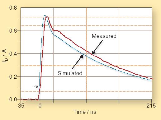
After a broadband bandpass filter in the Q band was designed, the circuit was tested using a test fixture. Several poles in the in-band response of the filter and the high insertion loss, caused by the double coaxial-to-microstrip transition, were observed. In order to eliminate all inaccuracies of the test method that masked the actual behavior of the circuit, and to obtain an accurate measurement up to 50 GHz, a coplanar to microstrip transition connected to a coplanar probe station was used.  Using the coplanar to microstrip transition to test the filter, the tested results were quite close to the simulations.

Several microstrip broadband attenuators were designed with a topology that provides constant attenuation over broad bandwidth with good input and output matching, which requires a reliable test fixture. The use of coplanar transitions provided accurate measurements. One attenuator of 3 dB is shown in Figure 3a and the attenuation and matching tested.

In a circuit design, it is important to have an accurate model or characterization of the active device. Before designing some amplifiers in the Q band, an EC2612 GaAs pHEMT transistor was tested using the coplanar to microstrip transitions. The chip has internal via holes for the source connections to ground. The drain and gate were bonded with 17.5 micron gold wires and length 200 µm. The reflection S-parameters of the transistor for -10 dBm input power, drain voltage 2 V and a drain-to-source current 10 mA.
  • CPW probes
The issues for testing the new sizes and frequencies in electronics are handling, fixturing and vision. Handling is a problem because human hands do not have the dexterity called for by the smallest electronic components and assemblies. Fixtures that are "hand-sized," with their larger contacts and thereby looser tolerances, generate parasitics that hinder good quality testing. As for vision, the human eye is not calibrated to easily distinguish discrete pieces as small as 0201 component, for example, with enough clarity to perform tests on them.

A rule of thumb is that repeatable measurements require 1 mil (0.0254 mm) contact placement accuracy at 10 GHz. A general solution to the previously mentioned test issues that enables an engineer to achieve this rule of thumb accuracy involves:
  • CPW probes that provide an electrical reference plane at a precise point in space with precise planar contact, and are capable of quick and easy calibration.
  • The DUT holder must be secure, maneuverable and easy to load or unload.
  • The probe holding fixture should be rigid, repeatable and allow the flexible placement of probes.
The best CPW probes offer a wide range of planar contact styles, such as GSG, GS and SG. They offer a broad range of pitches from 75 µ to 2500 µ, controlled impedance, traceable calibration and relatively low cost. These probes are defined by bandwidth, e.g., 18 GHz, 40 GHz, up to 220 GHz and should be relatively low priced so that labs can afford to have probes with planar contacts precisely suited to their testing needs.

CPW probe calibration is most efficient when there is a standard calibration kit available with standard calibration procedures. These procedures work best when they are internal to the test equipment and offer open-short-load-through (OSLT), line-reflect-match (LRM) and through-reflect-line (TRL) calibration, are software controlled with the capability of using SOLR, multiline (NIST) and other protocols.

  • Probe stations/DUT holders
A good probe station is flexible, portable, and low-cost and has options available that allow lab personnel to meet the specific testing demands of their customers' components and assemblies. The stations listed in the following paragraphs are capable of handling a wide range of applications, including, but not limited to testing semiconductor devices, microwave packages, MIC components and doing small sample failure analysis.

A basic, low-cost probe station that meets the needs of many engineers and scientists is capable of movement in the X, Y and Z axes. This grade of instrument will typically enable one inch of travel in the X and Y axes and 50 mils of vertical movement in the Z axis. The station will have a platen approximately 7" × 12" (178 mm × 305 mm) supporting a stage of approximately 2" × 2" (51 mm × 51 mm). A vacuum hold down secures components on the platen without placing stress in any plane. Optics on this type of probe station are in the 10x+ power range, and a fixed-intensity fluorescent ring illuminator provides adequate lighting for many applications.

For the engineer or scientist who requires higher precision in a probe station that fits well in a personal workspace, the instrument of choice would be a compact manual probe station. This instrument, sometimes called a personal probe station, expands the features of the basic probe station. The stage size increases to 4.5 inches (114.3 mm) and travel in the X axis is 2.5 inches (63.5 mm) and in the Y axis is 4 inches (102 mm). An added feature of this class of probe station is travel up to 180° rotation in either direction. Standard optics have 7x-112x capability, and lighting is a fixed-intensity fluorescent ring illuminator.

A full-featured manual probe station offers the greatest range of capabilities to deal with the most demanding applications. This instrument gives the engineer or scientist a choice of a 6.5 inch (165 mm) or 8.5 inch (216 mm) stage. Added weight and size give this model more stability during tests. Movement in the X and Y axes is a full 6 inch (152.4 mm), 0.25 inches (6.4 mm) Z lift, and 180° rotation in the . Zoom optics have a 0.7x-4x objective lens providing magnification of 42x-270x for probe placement and DUT alignment with the standard 0.5x auxiliary lens. Removal of the auxiliary lens changes the range of magnification to 84x-540x for inspection and fine geometry probing. There is a 2x relay lens and a 0.5x or 1.0x (no lens) objective multiplier.

  • Typical applications
Many electronics devices can be tested in the different probe station models. Some of these applications fit one model better than another, but in general, the following devices can all be tested in a good quality probe station.
First-order devices (do not require fixturing):
  • Semiconductors — GaAs or any other advanced IC, II-VI or III-V devices for process control monitoring, RF performance or pulsed IV performance.
  • Surface-mount devices (SMD) — Micro BGAs, leadless carriers or leaded carriers such as a standard SOIC, upside down on either a conductive or non-conductive chuck.
  • SMD passive devices — Standard or custom calibration of hybrid couplers using a custom chuck.
  • MMIC packages — Capable of standard or custom calibration, often with a custom probe configuration and a custom device under test (DUT) holder.
  • Interconnect structures — Test high-performance PCBs for signal integrity, transition, impedance and parasitic elements.
Second-order devices (require fixturing with thin film adapter substrates):
  • Transistors — Modeling and evaluation.
  • Diodes, single-port devices.
  • Packages that cannot be tested with standard CPW.
  • Options
While a probe station usually comes equipped with standard features that are adequate for a majority of applications, sometimes it is necessary to add options that enable testing components with unusual requirements. Some of the options available for probe stations are:
Manipulator/probe holder — these are available in different sizes, prices and features.
The basic model has a magnetic-mount positioner with dovetail slides for dc and general-purpose ac microprobing use, and features X, Y and Z travel. It usually comes with several needles that can be used to secure parts for test. This entry-level model has a magnetic mount.
A slightly higher-priced model is available in which the slides are mounted on roller bearings for smoother X-Y travel and longer life. The engineer or scientist who buys this class of manipulator/probe holder can expect a 40 or 80 turns-per-inch positioner knob for precise placement of parts being tested, as well as somewhat greater travel capability in all axes than on the basic model. Knob planarity adjustment is another feature that is standard on this model. As with the basic model, a magnetic mount attaches it to the probe station.
Full-featured manipulator/holders have all the features listed in the previous models, but are bolt-mounted rather than magnet-mounted, giving them greater part holding strength and stability. They also offer greater movement in all axes.

Upgraded microscope system;
  • vision-capture ready;
  • video-camera ready;
  • magnification range of 6.7x -168x with optional 1.5x objective;
  • thermal stage;
  • temperature control range of -5 °C to +125 °C;
  • vacuum DUT hold down; and
  • PCB holder — allows the testing of double-sided PCBs with bottom-side clearance.
  • Conclusion
Using CPW probes for precise measurements raises the bar. Having quality microwave transitions removes the uncertainty of how accurate the test data is because they improve the test contacts' integrity and the methods for micro-component measurements. CPW adapter substrates expand the applications that are possible. Microstrip devices become testable. A standardized calibration procedure assures that the measurement data is precise, repeatable and there is cross-facility data correlation.

Publicado por: Jahir Alonzo Linares Mora C.I: 19769430 CRF
Bibliografia: http://rfdesign.com/microwave_millimeter_tech/passive_components/radio_coplanar_waveguide_probes/

Typical Matching Situations

It's relatively easy to design resistive terminations for waveguide and TEM structures that provide extremely wideband loads with Z=Zo of the transmission line. For situations where the loads must dissipate substantial power, thermal considerations come into play, and some form of conductive or convective cooling is necessary to prevent destruction of the load. In the extreme case, a long enough length of terminated lossy transmission line will present a high-power matched load to a transmission line of the same dimensions.
The going gets tough in cases where impedance matching is required to narrow-band elements such as antennas or to devices with substantial reactance and resistance levels that are much lower (or higher) than typical transmission lines.
An arbitrary impedance can, in principle, be matched at a single frequency by adding sufficient transmission line to move the impedance around the Smith chart until it lies on an admittance circle that passes through the center of the chart (g=20 millimhos or milliSiemens), then adding susceptance of the proper sign to move the combined admittance to the =0 point. The simplified Smith charts here show one of the two possible solutions for an arbitrary normalized impedance.

The other solution is

Although inconvenient to realize in transmission line format, there are two other solutions that are obtained by rotating the arbitrary impedance until it is on the 50 circle, then adding the proper series reactance to bring the resulting impedance to the 50 point.
Recall that a useful expression for the impedance of a lossless transmission line of characteristic impedance Zo with an arbitrary load ZL and electrical length tita is

This can be used in connection with a spreadsheet or other calculation aid to keep track of the real and imaginary parts with varying frequency.
But these are single-frequency solutions to the impedance matching problem. Because one of the major advantages of microwave usage is the opportunity to transmit substantial bandwidth, and because in practice one would hope to avoid a requirement for a unique circuit for each of the many frequencies in a typical 40% waveguide band, broadband solutions to the matching problem are valuable and sought-after.


Publicado por: Jahir Alonzo Linares Mora C.I: 19769430 CRF

Impedance Matching

Why Impedance Match?

A question often asked by people new to the microwave field is, "what is so important about impedance matching?" The answer is that this is one of the very few known and reliable operating conditions (the others, which are harder to implement and are position-dependent, and for which no power transfer is possible, are the short and open circuit).

Efficient power transfer is possible with other source and load impedances at a single frequency, but the ability to measure and adjust to known conditions is too difficult to be reliable. The other advantage of the matched load condition is that it uniquely removes the requirement for a specific reference plane.

Also, the power-handling capacity of a transmission line is maximum when it is "flat", i.e., operating at low SWR. Lastly, it is important to be able to interconnect a number of different components into a system, and the only way that can be done reliably and predictably is by constraining the reflection coefficients of the various interfaces through impedance matching. Multiple reflections can result in group delay variations that can produce undesired intermodulation in broadband systems.

As we have seen, the S-parameter matrix is especially useful for transmission line and waveguide situations, because the various parameters are defined for matched conditions.
This is extremely helpful in measurement of active devices, which may not be stable with
source or load l l=1 characteristic of a short or open termination.

The greatest amount of engineering time is spent in searching for ways to provide efficient impedance matching, especially to active circuit elements, so it pays to know some of the many useful impedance-matching methods and their limitations. Microwave instruments for measurement of impedance by way of direct measurement or S-parameters are among the most widely used tools of the microwave engineer.


Publicado por Jahir Alonzo Linares Mora C.I: 19769430 CRF
Bibliografia: http://puhep1.princeton.edu/

Isolator (microwave)

An isolator is a two-port device that transmits microwave or radio frequency power in one direction only. It is used to shield equipment on its input side, from the effects of conditions on its output side; for example, to prevent a microwave source being detuned by a mismatched load.

Non-reciprocity

An isolator in a non-reciprocal device, with a non-symmetric scattering matrix. An ideal isolator transmits all the power entering port 1 to port 2, while absorbing all the power entering port 2, so that to within a phase-factor its S-matrix is
S = \begin{pmatrix}   0 & 0 \\   1 & 0  \end{pmatrix}
To achieve non-reciprocity, an isolator must necessarily incorporate a non-reciprocal material. At microwave frequencies this material is invariably a ferrite which is biased by a static magnetic field. The ferrite is positioned within the isolator such that the microwave signal presents it with a rotating magnetic field, with the rotation axis aligned with the direction of the static bias field. The behaviour of the ferrite depends on the sense of rotation with respect to the bias field, and hence is different for microwave signals travelling in opposite directions. Depending on the exact operating conditions, the signal travelling in one direction may either be phase-shifted, displaced from the ferrite or absorbed.

Types 

  • Resonance absorption

In this type the ferrite absorbs energy from the microwave signal travelling in one direction. A suitable rotating magnetic field is found in the TE10 mode of rectangular waveguide. The rotating field exists away from the centre-line of the broad wall, over the full height of the guide. However, to allow heat from the absorbed power to be conducted away, the ferrite does not usually extend from one broad-wall to the other, but is limited to a shallow strip on each face. For a given bias field, resonance absorption occurs over a fairly narrow frequency band, but since in practice the bias field is not perfectly uniform throughout the ferrite, the isolator functions over a somewhat wider band. 

  • Using a circulator
 A circulator is a non-reciprocal three- or four-port device, in which power entering any port is transmitted to the next port in rotation (only). So to within a phase-factor, the scattering matrix for a three-port circulator is

S = \begin{pmatrix}   0 & 0 & 1\\   1 & 0 & 0 \\   0 & 1 & 0 \end{pmatrix}

A two-port isolator is obtained simply by terminating one of the three ports with a matched load, which absorbs all the power entering it. The biassed ferrite is part of the circulator. The bias field is lower than that needed for resonance absorption, and so this type of isolator does not require such a heavy permanent magnet. Because the power is absorbed in an external load, cooling is less of a problem than with a resonance absorption isolator.

An X band isolator consisting of a waveguide circulator with an external matched load on one port
Two isolators each consisting of a coax circulator and a matched load

Publicado por Jahir Alonzo Linares Mora C.I: 19769430 CRF
Bibliografia: http://en.wikipedia.org/wiki/Isolator_(microwave)