A monolithic integrated multiband PCN/PCS RF-bandpass filter manufactured on highly resistive silicon substrate with mode conversion and ESD protection is described. In order to analyze the ESD behavior of the filter, an ESD simulation model is presented and compared with measurement results.
Integrated passive devices such as resistors, capacitors, coils and transformers have been introduced by several companies
In order to protect integrated filter circuits from ESD, ESD devices are either placed as discrete circuits around the critical input/output pins or integrated with the filter onto the chip. The last concept leads to a cheaper and smaller PCB outline
For the development of RF filters, a compromise between RF performance and ESD protection must be found. The non-linearities of active ESD devices, for example, can cause intermodulation and degrade the RF performance.
The new RF bandpass filter with integrated impedance matching, mode conversion and ESD protection is manufactured with an extended silicon-copper technology that allows integration of active and passive components on a single die. In the following sections, an RF filter with excellent ESD protection and filter performance will be discussed, and an analytical HBM simulation setup for these filters will be introduced.
- Si-Cu technology
An existing silicon-copper technology for passive integration was extended in order to integrate passive and active elements on a high-resistive Si substrate. Figure 1 shows the cross-section of the layer sequence for a typical RF filter with monolithic integrated planar inductors, metal-insulator-metal (MIM) capacitors, and ESD diodes.

Figure 1. Cross-section of the chip with a three-layer copper metallization
embedded in SiO2.
embedded in SiO2.
Coils and transformers are implemented in three-layer copper metallization. Metal-1 has a thickness of 600 nm and is mainly applied to lead through the metallization from the inside to the outside of the coils. Metal-2 and metal-3 have thicknesses of 2500 nm and are used for adjusting the coils to the required inductance. Due to the performance limitation of the skin effect, these stacked coils can be used for RF applications above 1 GHz. For lower-frequency applications, an increase of the copper layer thickness would be necessary to improve the quality factor (Q) of the inductors substantially. The inductances of typical integrated coils are in the range of 0.5 nH to 35 nH, with corresponding Q factors between 10 GHz and 16 at 1 GHz. Maximum Q values of about 40 were measured at 3 GHz for a corresponding L value of 0.5 nH.
The Al2 O3 MIM capacitors, which are necessary for the implementation of on-chip resonators, are placed between metal-1 and metal-2. With the new dielectric material, high specific capacitance values of from 1.4 fF/µm2 to 1.8 fF/µm2 can be achieved leading to small capacitor dimensions and small outlines of the chip design. The values for the MIM capacitors are in the range of between 0.1 pF and 30 pF, with corresponding Q factors of 100 at 1 GHz.
- Bandpass filter with mode conversion
With the extended S technology, filters with low insertion loss and high harmonic suppression can be designed. An integration of filter elements and balun on-chip replaces a high number of external SMD components, leading to reduced board space and lower assembly costs. Further advantages compared to discrete solutions are smaller component tolerances of these integrated devices and a reduced assembly error rate.

Figure 2. Bandpass fi lter with mode conversion for PCN applications
consisting of passive elements (coils, transformers and MIM capacitors),
as well as active elements (ESD diodes).
consisting of passive elements (coils, transformers and MIM capacitors),
as well as active elements (ESD diodes).
The schematic of the implemented PCN/PCS bandpass filter (1710 MHz to 1910 MHz) with mode conversion from differential to single ended is shown in Figure 2. The filter consists of a symmetrical filter design based on several optimized LC resonators. The mode conversion is carried out with an integrated autotransformer with a coupling factor of 0.83.
We focused on a high common-mode suppression at the second harmonic, leading to a symmetrical filter design. This design reduces the influence of the grounding to the common-mode signal, which results in an excellent common-mode suppression of about -40 dB at the second harmonic. In addition, the symmetrical design allows implementation of a dc biasing network in the mirror plane of the filter, acting as a dc current supply typically used to drive the modulators of a transceiver. The bandpass filter itself is housed in a thin, small, and leadless package with dimensions of only 2.0 × 1.3 × 0.4 mm.
Coils and autotransformers were considered in the simulation tool by de-embedded S-parameter measurements and a Spice netlist generated by a simulation tool, respectively. The parameters of the autotransformer model are extracted from its geometrical structure by applying a numerical solver for the electric and magnetic fields.
Figure 3 and Figure 4 show the insertion loss versus frequency and the common-mode suppression of a harmonic PCN/PCS filter, respectively. The insertion loss within the passband (1710 MHz and 1910 MHz) is about -2.5 dB, with a corresponding ripple of only 0.2 dB.

Figure 3. Comparison of simulation and measurement results for the
differential mode of the bandpass fi lter.
differential mode of the bandpass fi lter.

Figure 4. Comparison of simulation and measurement results for the
common-mode suppression of the bandpass fi lter.
common-mode suppression of the bandpass fi lter.
The suppression of the third harmonic is below -40 dB and in good agreement with the simulation results.
Using an autotransformer instead of a simple LC balun leads to an improved common-mode suppression of -30 dB in the frequency range between 3 GHz and 6 GHz. However, the simulation and measurement results differ at higher frequencies because of the implemented autotransformer model, which is only valid up to half of the self-resonance of the autotransformer itself.
- ESD model
EOS and ESD damage affects device functionality and RF performance. Therefore, it is important to make thorough investigations concerning ESD protection, especially for the MIM capacitors, in order to guarantee the required ESD robustness.
Figure 5 shows a complete ESD simulation setup consisting of the implemented ESD model (HBM, MM or CDM), the parasitics of the measurement setup, and the device under test (DUT). The investigations are focused on HBM, with corresponding values for RM = 1500 Ω, CM = 100 pF, and LM = 0 nH 5 .


In order to investigate the ESD protection of the filter sub-circuits (LD || CD ), a simple ESD model was developed. First of all, parasitic board elements are neglected so that only the parameter for HBM and the filter sub-circuit are considered. For this case, a linear differential equation of third order with the general solution is obtained.
With the initial conditions for current and voltages, the vector x0 is given by (U0 , 0, 0)T .


Figure 6. Simulated voltage at the capacitor CD (1 pF) for an LC sub-circuit.
HBM model (U0 = 1 kV).
HBM model (U0 = 1 kV).
To investigate the complete ESD setup, the board parasitics must be determined and included in the circuit simulator. The parameter extraction for the board parasitics is carried out in the following manner: First, the measurement equipment is characterized by current discharge for different terminations (0 Ω and 500 Ω) for the DUT, with which the board elements can be determined. Figure 7 shows simulated and measured results for a shorted device under test.
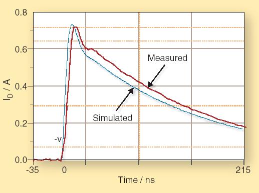
Figure 7. Measured and simulated results of the current discharge for a shorter device (Rd=0)
Transient simulations for the PCN/PCS bandpass filter with internal active and passive elements were carried out with the circuit simulator (ADS) from Agilent. Figure 8 shows the simulation results of the voltage drop for several MIM capacitors and reveals the endangered element for ESD damage.
- Conclusion
The performance of a monolithic integrated PCN/PCS RF bandpass filter with mode conversion, integrated dc power supply and ESD protection was discussed. Good RF filter performance in combination with ESD protection was achieved. The figure of merits of the RF filter are the insertion loss within the passband of -2.5 dB, the third harmonic suppression of -45 dB, the common mode suppression of -40 dB, and the ESD robustness of more than 3 kV.
Publicado por: Jahir Alonzo Linares Mora C.I: 19769430 CRF
Bibliografia: http://rfdesign.com/mag/611RFDF1.pdf
Publicado por: Jahir Alonzo Linares Mora C.I: 19769430 CRF
Bibliografia: http://rfdesign.com/mag/611RFDF1.pdf
No hay comentarios:
Publicar un comentario